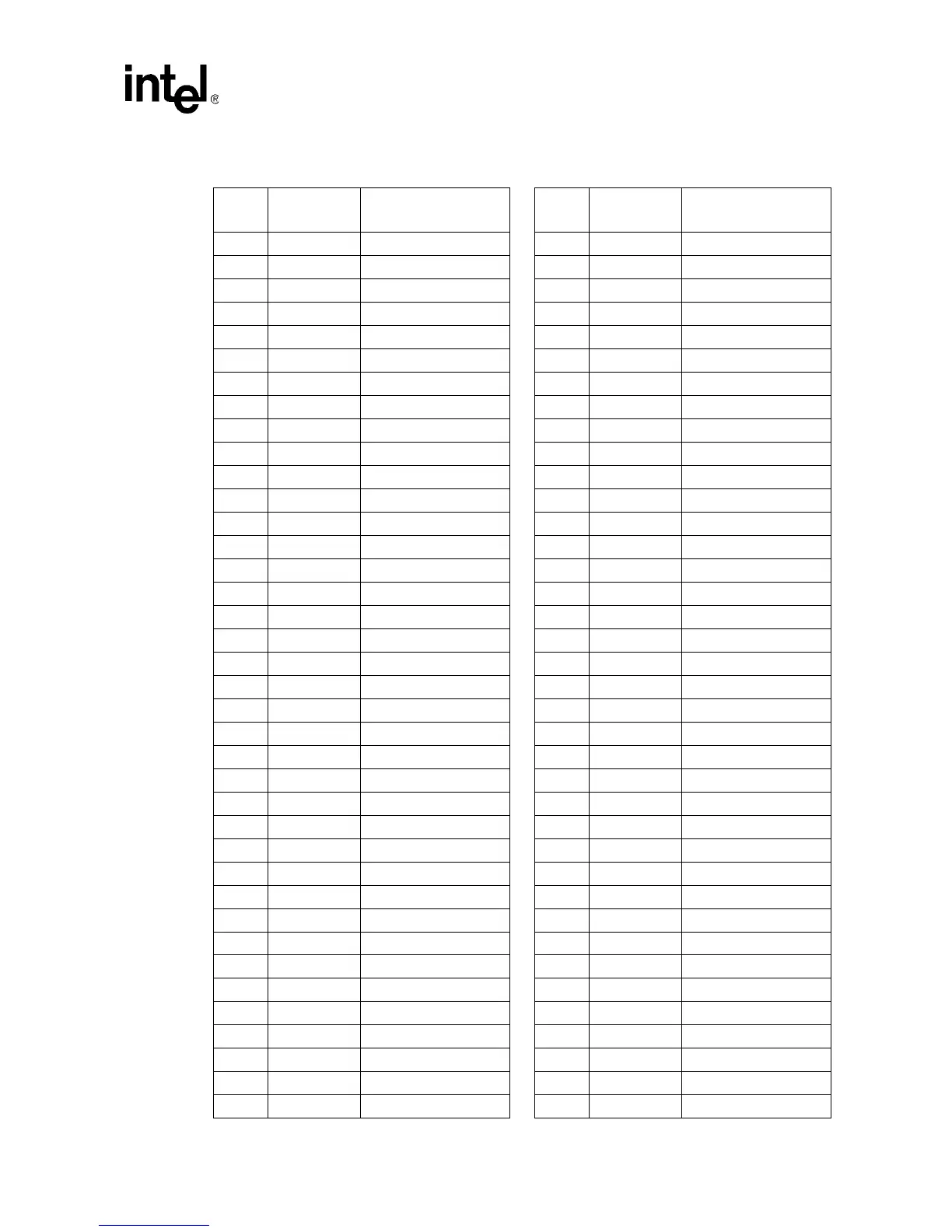
Datasheet 85
Intel
®
Celeron
®
Processor up to 1.10 GHz
E5 VCC
CORE
Power/Other
E7 V
SS Power/Other
E9 V
CC
CORE
Power/Other
E11 V
SS Power/Other
E13 V
CC
CORE
Power/Other
E15 V
SS Power/Other
E17 V
CC
CORE
Power/Other
E19 V
SS Power/Other
E21 V
CORE
DET
Power/Other
E23 Reserved Reserved for Future Use
E25 D62# Power/Other
E27 Reserved Reserved for Future Use
E29 Reserved Reserved for Future Use
E31 Reserved Reserved for Future Use
E33 V
REF0 Power/Other
E35 BPM1# AGTL+ I/O
E37 BP3# AGTL+ I/O
F2 V
CC
CORE
Power/Other
F4 V
CC
CORE
Power/Other
F6 D32# AGTL+ I/O
F8 D22# AGTL+ I/O
F10 Reserved Reserved for Future Use
F12 D27# AGTL+ I/O
F14 V
CC
CORE
Power/Other
F16 D63# AGTL+ I/O
F18 V
REF1 Power/Other
F20 V
SS Power/Other
F22 V
CC
CORE
Power/Other
F24 V
SS Power/Other
F26 V
CC
CORE
Power/Other
F28 V
SS Power/Other
F30 V
CC
CORE
Power/Other
F32 V
SS Power/Other
F34 V
CC
CORE
Power/Other
F36 V
SS Power/Other
G1 D21# AGTL+ I/O
G3 D23# AGTL+ I/O
G5 V
SS Power/Other
Table 49. PPGA Package Signal Listing
by Pin Number
Pin
No. Pin Name Signal Buffer Type
G33 BP2# AGTL+ I/O
G35 Reserved Reserved for Future Use
G37 Reserved Reserved for Future Use
H2 V
SS Power/Other
H4 D16# AGTL+ I/O
H6 D19# AGTL+ I/O
H32 V
CC
CORE
Power/Other
H34 V
SS Power/Other
H36 V
CC
CORE
Power/Other
J1 D7# AGTL+ I/O
J3 D30# AGTL+ I/O
J5 V
CC
CORE
Power/Other
J33 PICCLK APIC Clock Input
J35 PICD0 APIC I/O
J37 PREQ# CMOS Input
K2 V
CC
CORE
Power/Other
K4 V
REF2 Power/Other
K6 D24# AGTL+ I/O
K32 V
CC
CORE
Power/Other
K34 V
CC
CORE
Power/Other
K36 V
SS Power/Other
L1 D13# AGTL+ I/O
L3 D20# AGTL+ I/O
L5 V
SS Power/Other
L33 Reserved Reserved for Future Use
L35 PICD1 APIC I/O
L37 LINT1/NMI CMOS Input
M2 V
SS Power/Other
M4 D11# AGTL+ I/O
M6 D3# AGTL+ I/O
M32 V
CC
CORE
Power/Other
M34 V
SS Power/Other
M36 LINT0/INTR CMOS Input
N1 D2# AGTL+ I/O
N3 D14# AGTL+ I/O
N5 V
CC
CORE
Power/Other
N33 Reserved Reserved for Future Use
N35 Reserved Reserved for Future Use
Table 49. PPGA Package Signal Listing
by Pin Number
Pin
No. Pin Name Signal Buffer Type