These interfaces connect only to the HPS SDRAM subsystem so it is recommended to
use them in your design if the FPGA needs high-throughput, low-latency access to the
HPS SDRAM. The exception to this recommendation is if the FPGA requires cache
coherent access to SDRAM.
The FPGA-to-SDRAM interfaces cannot access the MPU ACP slave; so if you require a
master implemented in the FPGA to access cache coherent data, ensure that it is
connected to the FPGA-to-HPS bridge instead.
The FPGA-to-SDRAM interface has three port types that are used to create the AXI
and Avalon-MM interfaces:
• Command ports—issue read and/or write commands, and for receive write
acknowledge responses
• 64-bit read data ports—receive data returned from a memory read
• 64-bit write data ports—transmit write data
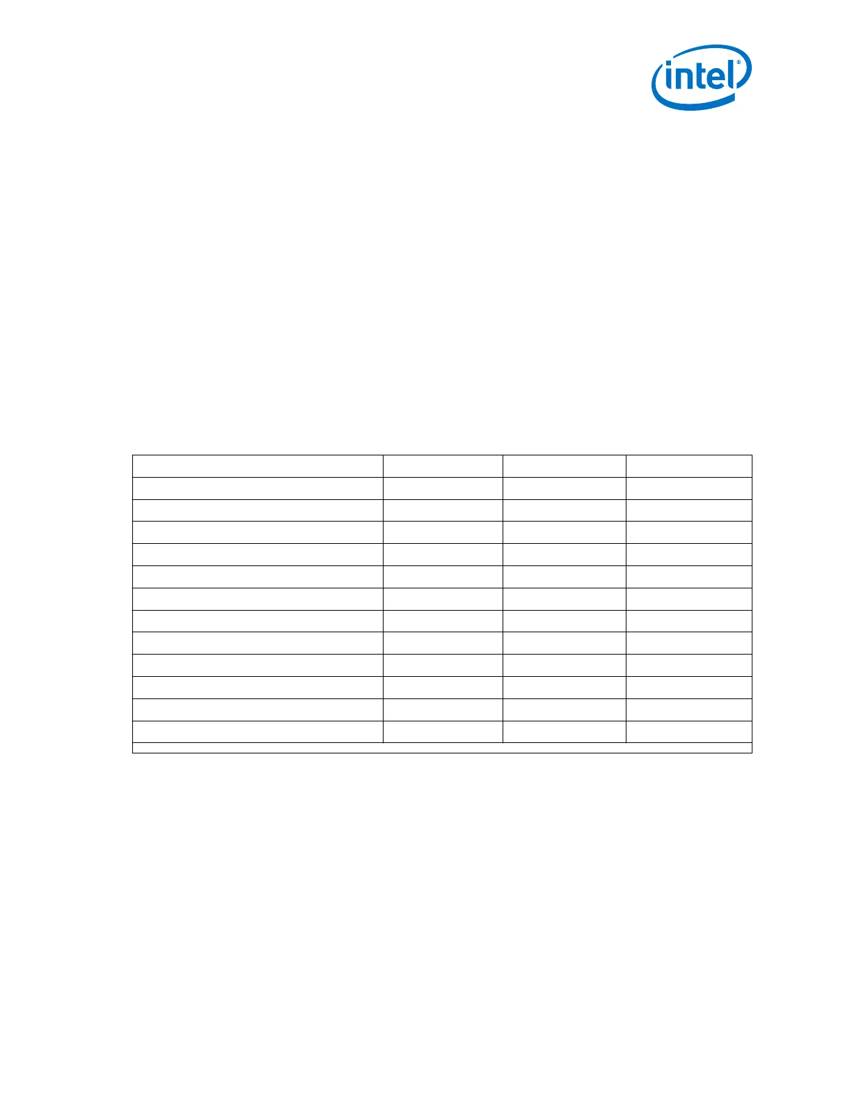
There is a maximum of six command ports, four 64-bit read data port and four 64-bit
write data port. The table below shows the possible port utilization.
Table 5. FPGA-to-HPS SDRAM Port Utilization
Bus Protocol Command Ports Read Data Ports Write Data Ports
32- or 64-bit AXI 2 1 1
128-bit AXI 2 2 2
256-bit AXI 2 4 4
32- or 64-bit Avalon-MM 1 1 1
128-bit Avalon-MM 1 2 2
256-bit Avalon-MM 1 4 4
32- or 64-bit Avalon-MM write-only 1 0 1
128-bit Avalon-MM write-only 1 0 2
256-bit Avalon-MM write-only 1 0 4
32- or 64-bit Avalon-MM read-only 1 1 0
128-bit Avalon-MM read-only 1 2 0
256-bit Avalon-MM read-only 1 4 0
For more information about the FPGA-to-HPS SDRAM interface, refer to the "SDRAM
Controller Subsystem" chapter of the Cyclone V or Arria V SoC Hard Processor System
Technical Reference Manual.
Note: To access the HPS SDRAM via the FPGA-to-SDRAM interface, follow the guidelines in
Access HPS SDRAM via the FPGA-to-SDRAM Interface on page 67.
Related Information
• SDRAM Controller Subsystem - Cyclone V Hard Processor System Technical
Reference Manual
• SDRAM Controller Subsystem - Arria V Hard Processor System Technical Reference
Manual
2. Background: Comparison between Cyclone V SoC FPGA and Arria V SoC FPGA HPS Subsystems
AN-796 | 2018.06.18
AN 796: Cyclone V and Arria V SoC Device Design Guidelines
13