1.1. The SoC FPGA Designer’s Checklist
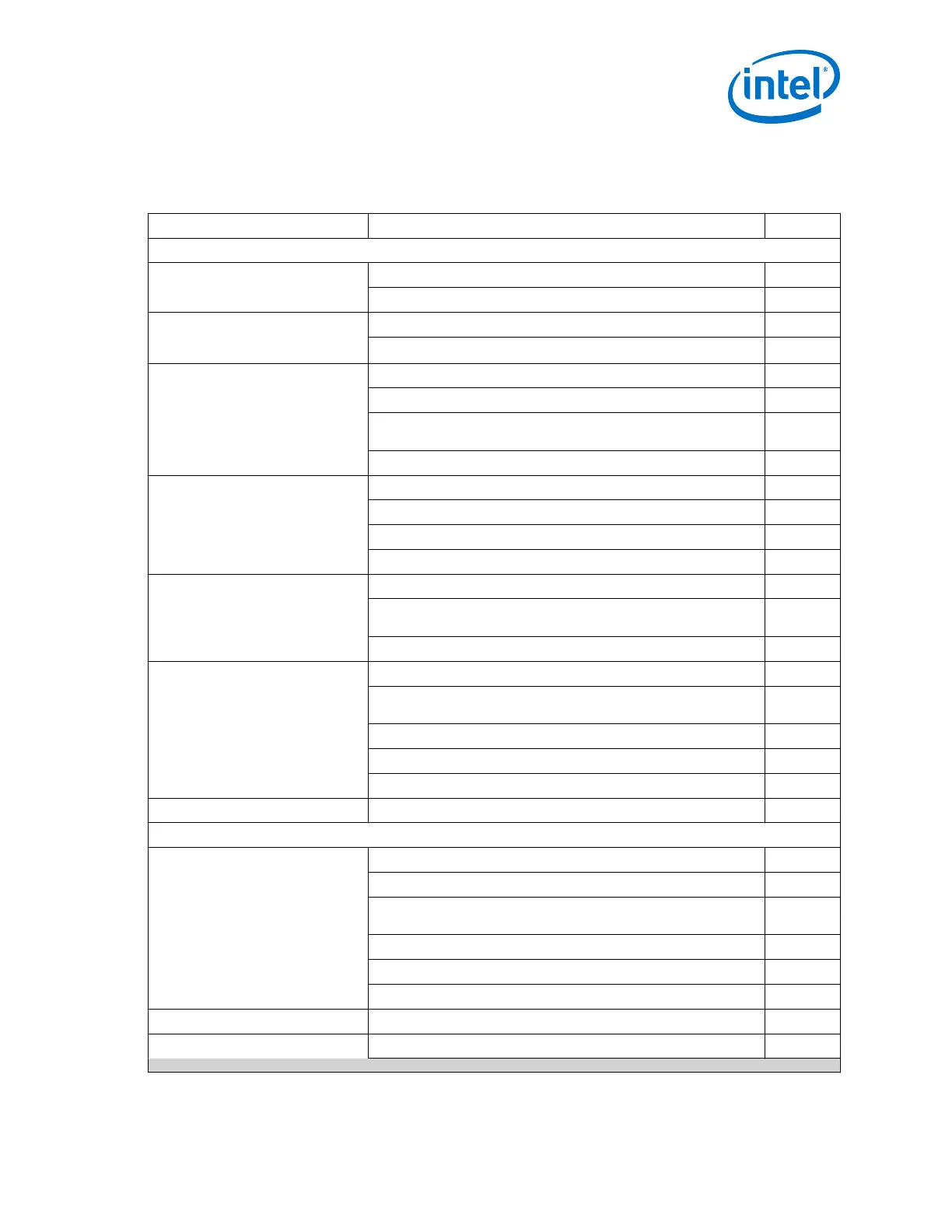
Table 1. The SoC FPGA Designer's Checklist
Step Title Links Check (X)
HPS Designer's Checklist for SoC FPGAs
Start your SoC FPGA Design here Start your SoC-FPGA design here on page 15
Determining your SoC FPGA Topology on page 15
Design Considerations for Connecting
Device I/O to HPS Peripherals and
Memory
HPS Pin Assignment Design Considerations on page 17
HPS I/O Settings: Constraints and Drive Strengths on page 18
HPS Clocking and Reset Design
Considerations
HPS Clock Planning on page 20
Early Pin Planning and I/O Assignment Analysis on page 20
Pin Features and Connections for HPS JTAG, Clocks, Reset and PoR
on page 20
Internal Clocks on page 21
HPS EMIF Design Considerations Considerations for Connecting HPS to SDRAM on page 21
HPS SDRAM I/O Locations on page 23
Integrating the HPS EMIF with the SoC FPGA Device on page 23
HPS Memory Debug on page 23
DMA Considerations Choosing a DMA Controller on page 24
Optimizing DMA Master Bandwidth through HPS Interconnect on page
24
Timing Closure for FPGA Accelerators on page 24
Managing Coherency for FPGA
Accelerators
Cache Coherency on page 25
Coherency between FPGA Logic and HPS: Accelerator Coherency Port
(ACP) on page 25
Data Size Impacts ACP Performance on page 25
FPGA Access to ACP via AXI or Avalon-MM on page 26
Data Alignment for ACP and L2 Cache ECC accesses on page 26
IP Debug Tools IP Debug Tools on page 26
Board Designer's Checklist for SoC FPGAs
HPS Power Design Considerations Early System and Board Planning on page 33
Early Power Estimation on page 33
Design Considerations for HPS and FPGA Power Supplies for SoC
FPGA devices on page 34
Pin Connection Considerations for Board Designs on page 34
Device Power-Up on page 34
Power Analysis and Optimization on page 35
Boundary Scan for HPS Boundary Scan for HPS on page 36
Design Guidelines for HPS Interfaces HPS EMAC PHY Interfaces on page 36
continued...
1. Overview of the Design Guidelines for Cyclone
®
V SoC FPGAs and Arria
®
V SoC FPGAs
AN-796 | 2018.06.18
AN 796: Cyclone V and Arria V SoC Device Design Guidelines
5