3.2. Design Considerations for Connecting Device I/O to HPS
Peripherals and Memory
One of the most important considerations when configuring the HPS is to understand
how the I/O is organized in the Cyclone V/Arria V SoC devices. The HPS I/O is
physically divided into:
• HPS Column I/O: Contains the HPS Dedicated Function Pins and HPS Dedicated
I/O with loaner capability
• HPS Row I/O: Contains the HPS External Memory Interface (EMIF) I/O and HPS
General Purpose Input (GPI) pins
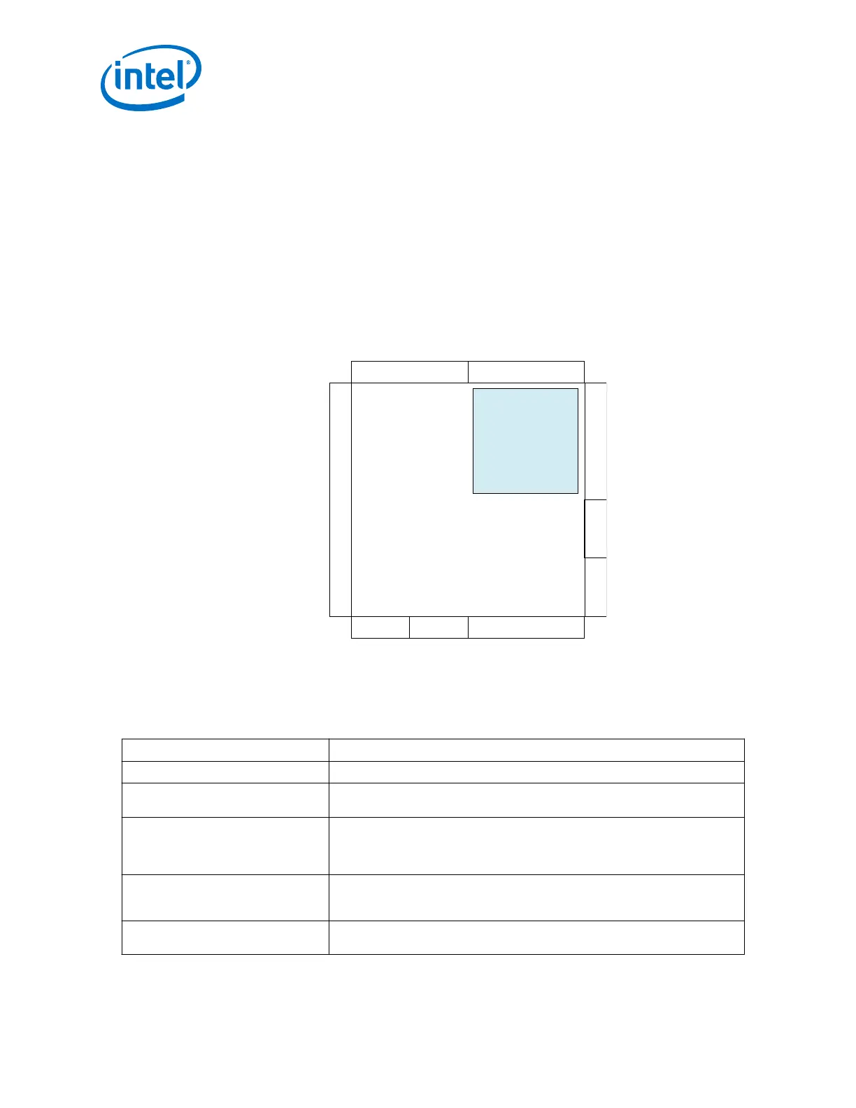
Figure 2. Example layout for HPS Column I/O and HPS Row I/O in Cyclone V SX and ST
device
Bank 8A HPS Column I/O
Bank 3B Bank 4ABank 3A
Bank 5B HPS Row I/OBank 5A
Transceiver Block
HPS Core
Note: For more information regarding the I/O pin layout, refer to the appropriate "I/O
Features" chapter in the Cyclone V or Arria V Device Handbook, Volume 1: Device
Interfaces and Integration.
Table 6. HPS I/O Pin Type Summary
Pin Type Purpose
HPS Dedicated Function Pins Each I/O has only one function and cannot be used for other purposes.
HPS Dedicated I/O with loaner
capability
These I/Os are primarily used by the HPS, but can be used on an individual basis
by the FPGA if the HPS is not using them.
HPS External Memory Interface (EMIF)
I/O
These I/Os are used for connecting to the HPS external memory interface
(EMIF). Refer to the "External Memory Interface in Cyclone V Devices" or
"External Memory Interface in Arria V Devices" chapter in the respective device
handbook for more information regarding the layout of these I/O pins.
HPS General Purpose Input (GPI) Pins These pins are also known as HLGPI pins. These input-only pins are located in
the same bank as the HPS EMIF I/O. Note that the smallest Cyclone V SoC
package U19 (484 pins) does not have any HPS GPI pins.
FPGA I/O These are general purpose I/O that can be used for FPGA logic and FPGA
External Memory Interfaces.
3. Design Guidelines for HPS portion of SoC FPGAs
AN-796 | 2018.06.18
AN 796: Cyclone V and Arria V SoC Device Design Guidelines
16