1.2. Overview of HPS Design Guidelines for SoC FPGA design
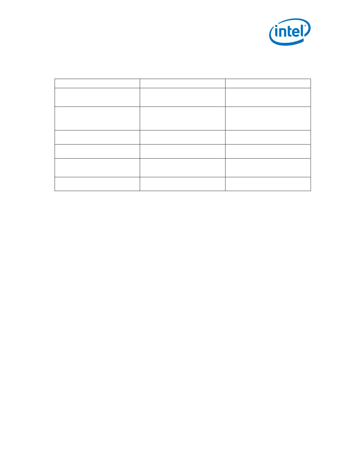
Table 2. HPS Design Guidelines Overview
Stages of the HPS Design Flow Guidelines Links
Hardware and Software Partitioning Determine your system topology and
use it as a starting point for your HPS
to FPGA interface design.
Guidelines for Interconnecting the HPS
and FPGA on page 10
HPS Pin Multiplexing and I/O
Configuration Settings
Plan configuration settings for the HPS
system including I/O multiplexing
options, interface to FPGA and SDRAM,
clocks, peripheral settings
Design Considerations for Connecting
Device I/O to HPS Peripherals and
Memory on page 16
HPS Clocks and Reset Considerations HPS clocks and cold and warm reset
considerations
HPS Clocking and Reset Design
Considerations on page 19
HPS EMIF Considerations Usage of the HPS EMIF controller and
related considerations
HPS EMIF Design Considerations on
page 21
FPGA Accelerator Design
Considerations
Design considerations to manage
coherency between FPGA accelerators
and the HPS
DMA Considerations on page 24
Recommended Tools for IP
Development
Signal Tap II, BFMs, System Console IP Debug Tools on page 26
1. Overview of the Design Guidelines for Cyclone
®
V SoC FPGAs and Arria
®
V SoC FPGAs
AN-796 | 2018.06.18
AN 796: Cyclone V and Arria V SoC Device Design Guidelines
7