Table of Contents Intel® Server Boards S3200SH/S3210SH TPS
Revision 1.3
iv
Table of Contents
1. Introduction ..........................................................................................................................1
1.1 Chapter Outline........................................................................................................ 1
1.2 Server Board Use Disclaimer .................................................................................. 1
2. Server Board Overview........................................................................................................2
2.1 Server Board Feature Set........................................................................................ 2
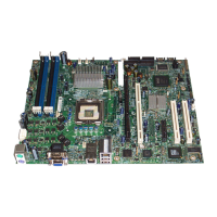
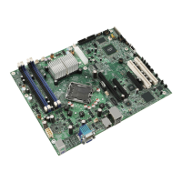
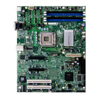
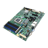
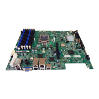
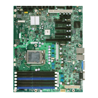
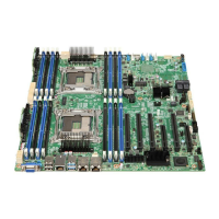
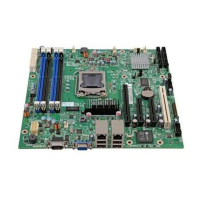
2.2 Server Board Layout.............................................................................................. 10
2.2.1 Server Board Mechanical Drawings ...................................................................... 11
3. Functional Architecture.....................................................................................................13
3.1 Processor Sub-System .......................................................................................... 16
3.1.1 Processor Voltage Regulator Down (VRD)............................................................ 16
3.1.2 Reset Configuration Logic ..................................................................................... 16
3.2 Intel
®
3200/3210 Chipset ....................................................................................... 17
3.2.1 Intel
®
3200/3210 Chipset MCH: Memory Control Hub...........................................17
3.2.2 PCI-X* Hub (PXH)..................................................................................................20
3.2.3 Intel
®
ICH9R: I/O Controller Hub 9R ......................................................................21
3.3 Memory Sub-System ............................................................................................. 27
3.3.1 Memory Configuration ........................................................................................... 27
3.3.2 Memory DIMM Support.......................................................................................... 30
3.4 I/O Sub-System .....................................................................................................30
3.4.1 PCI Subsystem ...................................................................................................... 30
3.4.2 Interrupt Routing .................................................................................................... 32
3.5 BMC Controller ......................................................................................................37
3.6 PCIe* to PCI-X* Bridge 6702PXH (PXH-V) (LX Board SKU Only) ........................ 38
3.7 Clock Generator..................................................................................................... 39
3.8 Super I/O ............................................................................................................... 39
3.9 GigE Controller 82541PI........................................................................................39
3.10 GigE PHY ..............................................................................................................40
3.11 On Board Components .......................................................................................... 40
3.11.1 Video Support ........................................................................................................ 40
3.12 Replacing the Back-Up Battery.............................................................................. 42
4. System BIOS.......................................................................................................................43
4.1 BIOS Identification String....................................................................................... 43
 Loading...