mP4G/mP4GL Series Motherboard
○○○○○○○○○○○○○○○○○○○○○○○○○○○○○○○○○○○○○○○○○○○○○○○○○○
User’s Manual
2•22
○○○○○○○○○○○○○○○○○○○○○○○○○○○○○○○○○○○○○○○○○○○○○○○○○○
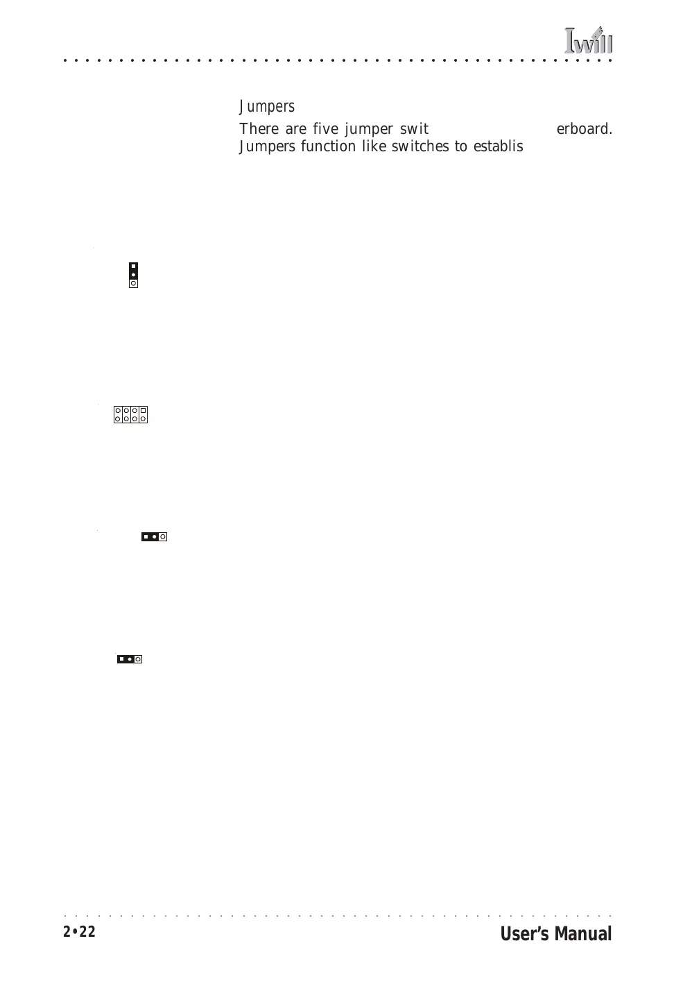
Jumpers
There are five jumper switches on this motherboard.
Jumpers function like switches to establish a hardware
configuration setting.
JCMOS1 Clear CMOS
Function: Clears the CMOS Setup Utility configuration
record stored in the real-time clock’s CMOS memory.
Description: A 3-pin jumper. Default Setting: Normal
More Information: See Chapter 3 for configuration in-
formation and the Troubleshooting section in Chapter 6.
JDIMMVOLT1 DDR Voltage
Function: Sets the voltage supplied to the DIMM DDR
memory sockets.
Description: An 8-pin jumper. Default Setting: 2.5V
More Information: See Chapter 3 for configuration in-
formation and “System Features” in Chapter 6.
JUSBV1 USB Standby Voltage
Function: Sets the voltage status for the USB ports.
Description: A 3-pin jumper. Default Setting: 5V
More Information: See Chapter 3 for information on con-
figuring this jumper.
JPSKMV1 PS/2 Standby Voltage
Function: Sets the voltage status for the PS/2 ports.
Description: A 3-pin jumper. Default Setting: 5V
More Information: See Chapter 3 for information on con-
figuring this jumper.
JDIMMVOLT1
JUSBV1
JPSKMV1
JCMOS1
JCMOS1 Clear CMOS:
Default – Normal
JDIMMVOLT1
DDR Voltage:
Default – 2.5V
JUSBV1 USB Voltage:
Default – 5V
JPSKMV1 PS/2 Voltage:
Default – 5V
Pin 1
Pin 8
Pin 7
Pin 2
Pin 1
Pin 1
Pin 1