P/N 960-000180R_Rev. 1 {EDP #233427} © 2016, JAPAN CASH MACHINE CO., LTD.
Installation DBV® Series DBV-400 Banknote Validator Section 2
Standard Interface Circuit Schematics
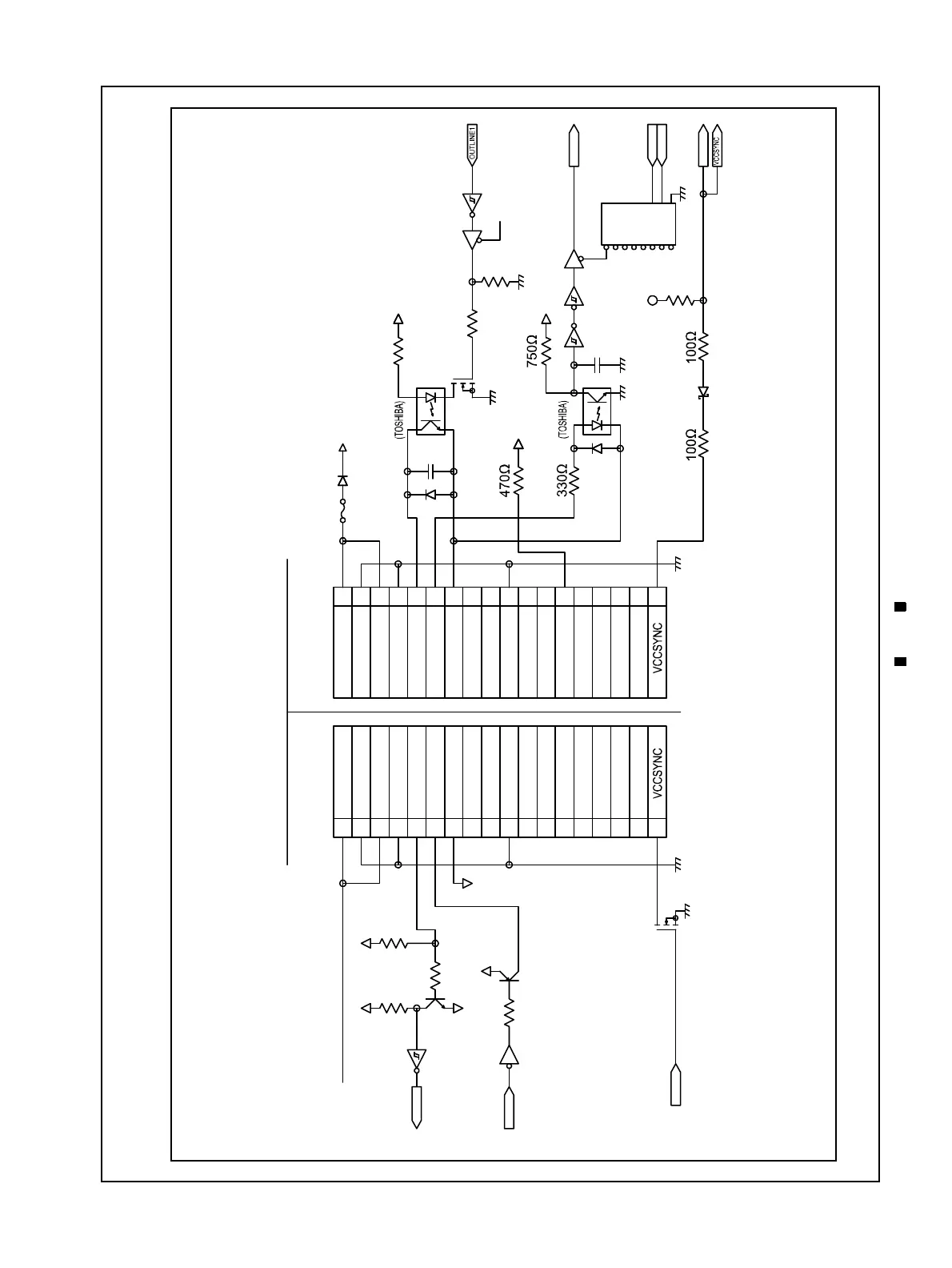
Figure 2-11 illustrates the DBV-400 ID-003 MDB/Photo-Coupler Isolation Interface Schematic Diagram.
Figure 2-11 DBV-400 ID-003/MDB Photo-Coupler Isolation Interface Schematic Diagram
Figure 2-11 DBV-400 ID-003/MDB Photo-Coupler Isolation Interface Schematic Diagram
Power
Power
5V
1
2
3
4
5
6
7
8
9
10
11
12
13
14
15
16
17
18
1
2
3
4
5
6
7
8
9
10
11
12
13
14
15
16
17
18
IN12V-24V
GND
IN12V-24V
GND
TXD
Common
GND
IN12V-24V
GND
IN12V-24V
GND
TXD
Common
GND
TLP781
5V
100pF
1SS352
5V
3.3V
TLP781
1SS352
100pF
3.3V
100K
1SS357
Sleep Control
INLINE1
IFSEL1
IFSEL2
WAKEUP
Y0
Y1
Y2
Y3
Y4
Y5
Y6
Y7
A
B
C
RXDRXD
CONTROLLER SIDE
DBV-400 SIDE