P/N 960-000180R_Rev. 1 {EDP #233427} © 2016, JAPAN CASH MACHINE CO., LTD.
Installation DBV® Series DBV-400 Banknote Validator Section 2
Standard Interface Circuit Schematics (Continued 6)
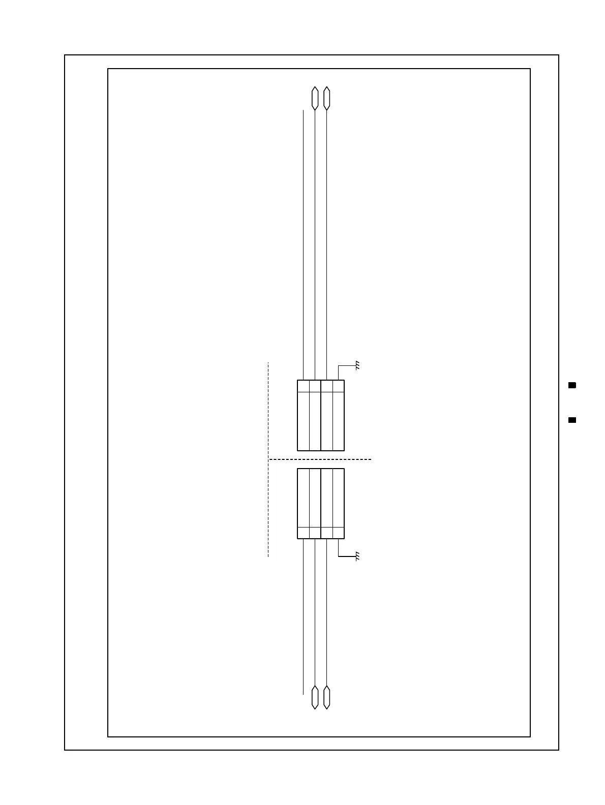
Figure 2-17 illustrates the DBV-400 USB Interface Schematic Diagram.
Figure 2-17 DBV-400 USB Interface Schematic Diagram
Figure 2-17 DBV-400 USB Interface Schematic Diagram
Vbus
Vbus
D-
D+
GND
1
2
3
4
Vbus
D-
D+
GND
1
2
3
4
Vbus
D -
D +
D -
D +
CONTROLLER SIDE
DBV-400 SIDE