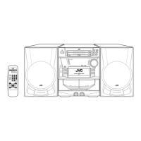
MX-J170V
1-29
–
+
+
–
1
2
3
4
8
7
6
5
OUT1
– IN1
+ IN1
V
EE
VCC
OUT2
– IN2
+ IN2
1ch
2ch
BA4560 (UIC1) / KA4558 (DIC2) : Dual OP AMP
1.Pin layout
1
2
3
4
5
NC
IN A
GND
Vcc
OUT Y
TC7SU04F (C12) : Inverter
SymbolPin.No
Function
P31
Parallel converts darta output terminals
Parallel converts darta output terminals
Parallel converts darta output terminals
P42
P53
4
P65
P76
Ground
Power supply terminal
P87
DATA8 Serial data input termnal
Clock signal input termnal
Strove signal input termnal
Clear signal input termnal
CLK9
STB10
CLR11
P1
P2
12
V
DD
V
SS
13
14
1
2
3
4
5
6
7
8
14
13
12
11
10
9
P3
P2
P1
CLR
STB
CLK
DATA
P4
P5
P6
P7
P8
V
DD
V
SS
NJU3711M (UIC2) : 8-BIT Serial to parallel conveter
1. Pin layout
2. Pin function
Description of major ICs