MachXO2 and MachXO3 Starter Kit Evaluation Board User Guide
Evaluation Board User Guide
© 2014-2022 Lattice Semiconductor Corp. All Lattice trademarks, registered trademarks, patents, and disclaimers are as listed at www.latticesemi.com/legal.
All other brand or product names are trademarks or registered trademarks of their respective holders. The specifications and information herein are subject to change without notice.
12 FPGA-EB-02036-1.4
6. Demonstration Design
Lattice provides a simple, pre-programmed demo to illustrate basic operation of the MachXO2 and MachXO3 devices.
The design integrates an up-counter with the on-chip oscillator. For the XO3L Starter Kit, pre-programmed design
resides in the external Serial Flash Memory (SPANSION S25FL204K or S25FL208K, or ON Semiconductor LE25U40CMD).
For the XO2 and XO3LF Starter Kits, the pre-programmed design resides in the on-board configuration flash memory.
Note: To restore the factory default demo and program it with other Lattice-supplied examples see the Download
Demo Designs section.
Overview
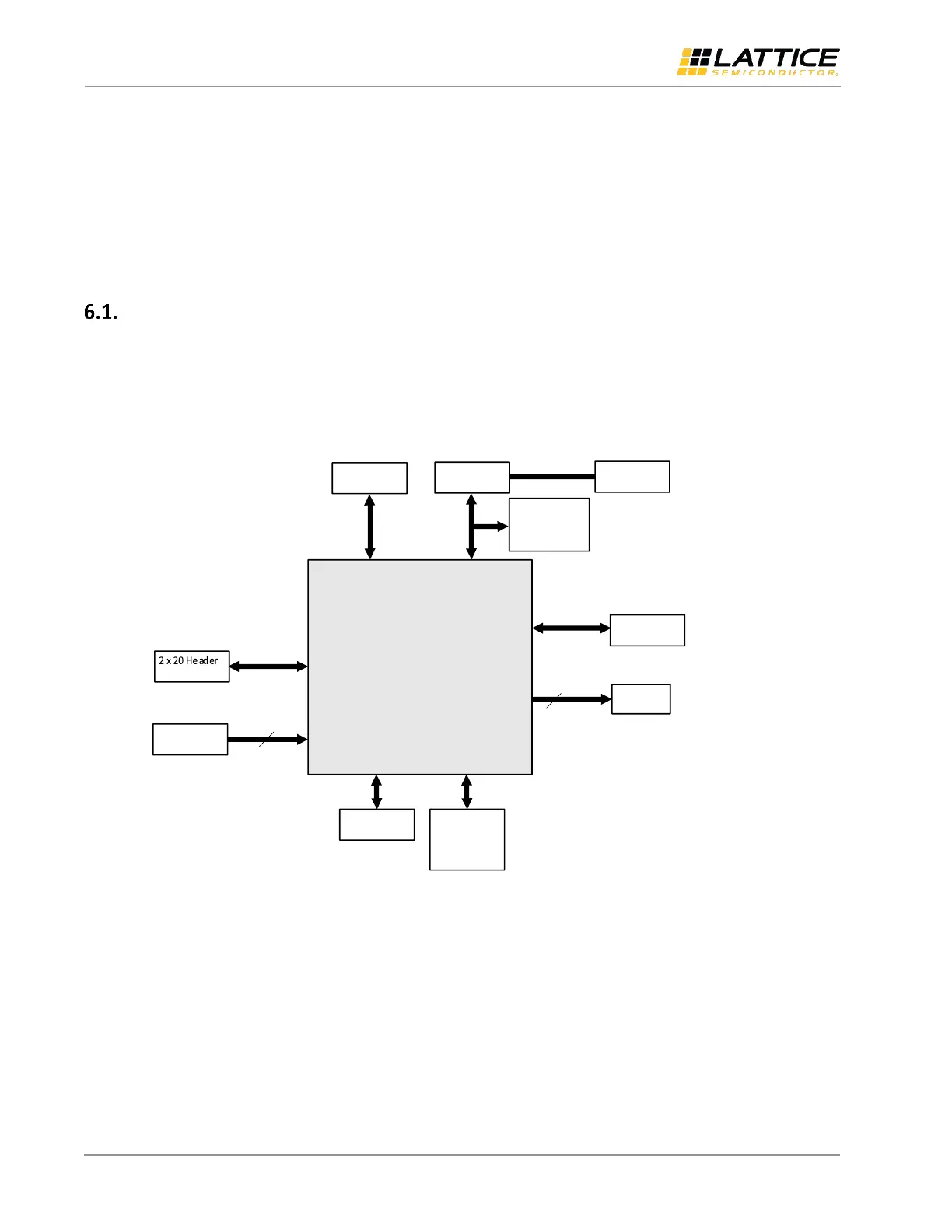
The Starter Kit is a complete development platform for the MachXO2 and MachXO3 FPGAs. The board includes a
prototyping area, a USB program/power port, an LED array, switches, and header landings with electrical connections
to most of the FPGA’s programmable I/O, power, and configuration pins. The board is powered by the PC’s USB port or
optionally with external power. You may create or modify the program files and reprogram the board using Lattice
Diamond software.
MachXO3L/LF-6900C device
2 x 20 Header
Landing (J6)
LED
Array
GPIO
8
2 x 20 Header
Landing (J3)
GPIO
2 x 20 Header
Landing (J4)
Bank 1
Bank 2
Bank 0
Landing (J8)
Bank 3, 4 and 5
GPIO
GPIO
USB
Controller
USB Mini B
Socket
1 x 8 Header
Landing (J1,
Optional JTAG
Interface)
JTAG
Programming
1 x 6 Header
Landing (J7,
Optional SPI,
I
2
C Intrfaces)
Bank 0, 2
DIP_SW
4
Figure 6.1. MachXO2 and MachXO3L/LF-6900C Block Diagram
 Loading...