MachXO2 and MachXO3 Starter Kit Evaluation Board User Guide
Evaluation Board User Guide
© 2014-2022 Lattice Semiconductor Corp. All Lattice trademarks, registered trademarks, patents, and disclaimers are as listed at www.latticesemi.com/legal.
All other brand or product names are trademarks or registered trademarks of their respective holders. The specifications and information herein are subject to change without notice.
FPGA-EB-02036-1.4 29
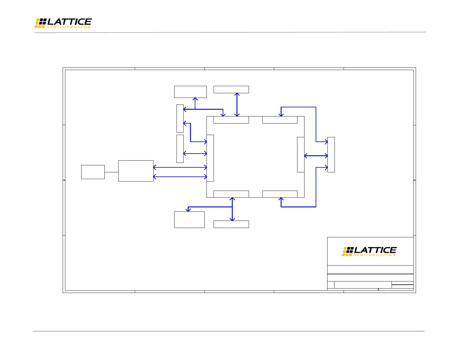
Appendix A. Schematic Diagrams
Figure A.1. Block Diagram
5
5
4
4
3
3
2
2
1
1
D D
C C
B B
A A
USB
CONNECTOR
USB to
JTAG / RS232
Power from USB 5V
BANK-1 BANK-5
BANK-4BANK-2
BANK-0
LCMXO3L/LF-6900C-5BG256C
JTAG_I/F
HEADER
HEADER
I/O'S
I2C
I/O'S
I/O'S
I/O'S
HEADER
I/O'S
I/O'S
BANK-3
HEADER
RS232_I/F
LEDS (1-8)
SPI FLASH
HEADER
SPI
Date:
Size
Schematic Rev
of
Sheet
Title
Lattice Semiconductor Applications
Email: techsupport@Latticesemi.com
Phone (503) 268-8001 -or- (800) LATTICE
Board Rev
12-SEP-2014
B
1.0
8
1
MACHXO3 Starter Kit - BLOCK DIAGRAM
Project
MACHXO3 Starter Kit - LCMXO3L-6900C
A