MachXO2 and MachXO3 Starter Kit Evaluation Board User Guide
Evaluation Board User Guide
© 2014-2022 Lattice Semiconductor Corp. All Lattice trademarks, registered trademarks, patents, and disclaimers are as listed at www.latticesemi.com/legal.
All other brand or product names are trademarks or registered trademarks of their respective holders. The specifications and information herein are subject to change without notice.
FPGA-EB-02036-1.4 13
Table 6.1 describes the components on the board and the interfaces it supports.
Table 6.1. Starter Kit Components and Interfaces
USB-to-JTAG interface and dual USB UART/FIFO IC
Programming and debug interface
LCMXO2, LCMXO3L, or
LCMXO3LF
U5: LCMXO2-
4000ZE-1BG256C,
LCMXO3L-6900C-
5BG256C or
LCMXO3LF-
6900C-5BG256C
4000-LUT and 6900-LUT devices are in a 14 mm x 14 mm,
256-ball caBGA package.
Four 2 x 20 Header
Landings
J3: header_2x20
J4: header_2x20
J6: header_2x20
J8: header_2x20
Optional SPI/I
2
C interfaces
4 x 10 40-Hole Prototype
Area
Prototype area 100 mil centered holes.
TP1: +3.3 V TP2:
+1.2 V TP3: GND
Power and ground reference points
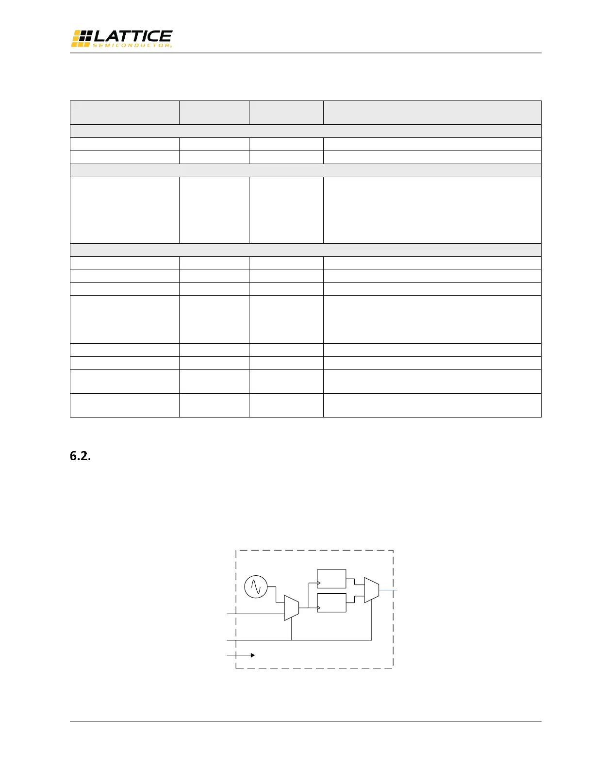
Run the Demonstration Design
Upon power-up, the pre-programmed demonstration design automatically loads and drives the LED array in a 1-hertz
pattern. The program shows a clock divider driven either by the MachXO2/MachXO3 internal oscillator or the external
FTDI clock chip. The divider modules (heartbeat.v and kitcar.v) are clocked at the default frequency of 12 MHz which
divides the clock to cycle the LED display approximately once per second. The resulting light pattern is determined by
the DIP Switch (SW2) setting as shown in Table 6.2.
MachXO3
X1
12.0 MHz
OSCH
12.09 MHz
Kitcar.v
Heartbe at.v
SW2
4-Position DIPSW
1 x 8
LED
Array
XO3L_SK_blink.v
SW1
Momentary PB
Async Reset
Figure 6.2. Demonstration Design Block Diagram
 Loading...