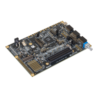
MachXO2 and MachXO3 Starter Kit Evaluation Board User Guide
Evaluation Board User Guide
© 2014-2022 Lattice Semiconductor Corp. All Lattice trademarks, registered trademarks, patents, and disclaimers are as listed at www.latticesemi.com/legal.
All other brand or product names are trademarks or registered trademarks of their respective holders. The specifications and information herein are subject to change without notice.
24 FPGA-EB-02036-1.4
Table 7.8. JTAG Programming Pin Information
Table 7.9. SPI Programming Pin Information
Master Clock/Config Clock
Table 7.10. I
2
C Programming Pin Information
LEDs
A blue LED (D1) is used to indicate USB 5V power. Eight red LEDs are driven by I/O pins of the MachXO2/MachXO3
device.
Table 7.11. Power and User LEDs Reference
Red LEDs (D2, D3, D4, D5, D6, D7, D8, D9) Blue LEDs (D1)
LTST-C190KRKT (D2-D9) LTST-C190TBKT (D1)
Power Supply
3.3 V and 1.2 V power supply rails are converted from the USB 5 V interface when the board is connected to a host
PC.
Test Points
In order to check the various voltage levels used, the following test points are provided:
• TP1: +3.3 V
• TP2: +1.2 V
• TP3: GND
USB Programming and Debug Interface
The USB Mini-B socket of the Starter Kit serves as the programming and debug interface. For JTAG programming, a pre-
programmed USB PHY peripheral controller is provided on the Starter Kit to serve as the programming interface to the
MachXO2/MachXO3 FPGA. Programming requires the Lattice Diamond or ispVM System software.

 Loading...