MachXO2 and MachXO3 Starter Kit Evaluation Board User Guide
Evaluation Board User Guide
© 2014-2022 Lattice Semiconductor Corp. All Lattice trademarks, registered trademarks, patents, and disclaimers are as listed at www.latticesemi.com/legal.
All other brand or product names are trademarks or registered trademarks of their respective holders. The specifications and information herein are subject to change without notice.
FPGA-EB-02036-1.4 23
LCMXO2-700 0HE4TG144C
D9 LED0
D8 LED1
D7 LED2
D6 LED3
D5 LED4
D4 LED5
D3 LED6
D2 LED7
H11
LED Net
LED Array
MachXO2/
MachXO3 Ball
J13
J11
L12
K11
L13
N15
P16
Top Side
TCK
GND
TMS
nc
nc
TDI
TDO
VCCIO0
8
1
J1
J1
J7
D9
D2
DIP_SW4
DIP_SW1
MCLK
SISPI
SPISO
SN
SCL
SDA
6
1
J7
DIP_SW1
DIP_SW2
DIP_SW3
DIP_SW4
N2
Net
MachXO2/
MachXO3 Ball
P1
M3
N1
SW2
Figure 7.3. J1 Header Landing and LED Array Callout
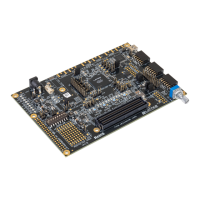
MachXO2/MachXO3 FPGA
The LCMXO2-4000ZE-1BG256C and LCMXO3L/LF-6900C-5BG256C are 256-ball caBGA package FPGA devices which
provide up to 206 usable I/O in a 14 mm x 14 mm package. 150 I/O are accessible from the board headers, switches,
and LEDs.
Table 7.6. MachXO2 and MachXO3 FPGA Interface Reference
LCMXO2-4000ZE-1BG256C (Flash),
LCMXO3L-6900C-5BG256C (NVCM) or
LCMXO3LF-6900C-5BG256C (Flash)
Programming Interface Circuits
For power and programming an FTDI USB UART/FIFO IC converter provides a communication interface between a
PC host and the JTAG programming chain of the Starter Kit. The USB 5 V supply is also used as a source for the
3.3 V supply rail. A USB mini-B socket is provided for the USB connector cable.
Table 7.7. USB/JTAG Interface Reference
Future Technology Devices International (FTDI)

 Loading...