MachXO2 and MachXO3 Starter Kit Evaluation Board User Guide
Evaluation Board User Guide
© 2014-2022 Lattice Semiconductor Corp. All Lattice trademarks, registered trademarks, patents, and disclaimers are as listed at www.latticesemi.com/legal.
All other brand or product names are trademarks or registered trademarks of their respective holders. The specifications and information herein are subject to change without notice.
FPGA-EB-02036-1.4 25
Table 7.12. USB Interface Reference
Future Technology Devices International (FTDI)
Board Modifications
This section describes modifications to the board to change or add functionality.
Bypassing the USB Programming Interface
The USB programming interface circuit (USB Programming and Debug Interface section) may be optionally bypassed by
removing the 0 Ω resistors: R4, R5, R6, R7 (See Figure A.2). Header landing J1 provides JTAG signal access for jumper
wires or a 1 x 8 pin header.
Applying External Power
The Starter Kit is powered by the circuit shown in Figure A.3, based on the 5 V USB power source. You may disconnect
this power source by removing the 0 Ω resistors: R35 (VCC_1.2 V) and R42 (VCC_3.3 V). Power connections are
available from the test points, TP1 (+3.3 V) and TP2 (+1.2 V). When this power mode is used, the FTDI oscillator will be
shut off.
Measuring Bank and Core Power
Test points (TP1, TP2) provide access to power supplies of the MachXO2/MachXO3 FPGA. Inline 1 Ω resistors: R31
(VCCIO0, +3.3 V, Bank 0), R25 (VCCIO1, +3.3 V, Bank 1), R37 (VCCIO2, +3.3 V, Bank 2), R32 (VCCIO3, +3.3 V, Bank 3), R26
(VCCIO4, +3.3 V, Bank 4), R38 (VCCIO5, +3.3 V, Bank 5), R24 (VCC core, +1.2 V) can be used to measure current for the
power supplies.
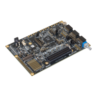
Mechanical Specifications
Dimensions: 3 in. [L] x 3 in. [W] x 1/2 in. [H]
Environmental Requirements
The evaluation board must be stored between -40° C and 100° C. The recommended operating temperature is between
0° C and 90° C.