MachXO2 and MachXO3 Starter Kit Evaluation Board User Guide
Evaluation Board User Guide
© 2014-2022 Lattice Semiconductor Corp. All Lattice trademarks, registered trademarks, patents, and disclaimers are as listed at www.latticesemi.com/legal.
All other brand or product names are trademarks or registered trademarks of their respective holders. The specifications and information herein are subject to change without notice.
FPGA-EB-02036-1.4 31
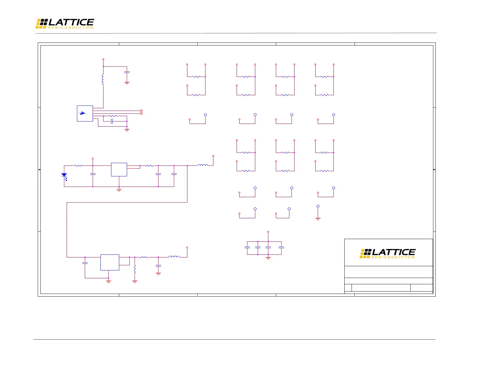
Figure A.3. FPGA
5
5
4
4
3
3
2
2
1
3
D D
C C
B B
A A
NOTE : Boot from external SPI Flash (U6)
requires VCCIO2 set to 3.3V. Use caution when
setting VCCIO2 to any other voltage.
VBUS_5V
+ 3.3V
+ 1.2V
VBUS_5V
+ 3.3V VCCIO0
+ 1.2V
+ 3.3V VCCIO3
+ 1.2V
+3.3V VCCIO1
+1.2V
+3.3V VCCIO4
+1.2V
+ 3.3V
VCCI
O2
+ 1.2V
+ 3.3V VCCIO5
+ 1.2V
+ 3.3V VCC_CORE
+3.3V
VCCIO3 VCCIO4 VCCIO5
VCC_CORE VCCIO0 VCCIO1 VCCIO2
+ 3.3V +1.2V
+ 1.2V
DM Sheet[2]
DP Sheet[2]
R42 0
R26 1
TP6
1
L3
600ohm 500mA
12
R31 1
L4
600ohm 500mA
12
C18
22uF
C62
1uF
R37 1
C20
22uF
TP9
1
TP7
1
R29 1
DNI
TP1
1
U4
NCP1117
GND
1
IN
3
OUT
2
TAB
4
C17
10uF
L5
600ohm 500mA
12
TP10
1
D1
Blue
12
R33 1
DNI
TP8
1
R86 1
DNI
R39 1
DNI
C21
0.1uF
TP3
1
C15
0.1uF
TP5
1
TP11
1
R32 1
TP2
1
R25 1
C64
0.01uF
U3
FAN1112
GND
1
Output
2
Input
3
Tab
4
J2
SKT_MINIUSB_
B_RA
VCC
1
D-
2
D+
3
ID
4
GND
5
R41
1K
C61
10uF
R38 1
C16 0.1uF
R35 0
C19
10uF
C63
0.1uF
R30 0
R34 1
DNI
R36
100
R28 1
DNI
R24 1
R40 1
DNI
Date:
Size
Schematic Rev
of
Sheet
Title
Lattice Semiconductor Applications
Email: techsupport@Latticesemi.com
Phone (503) 268-8001 -or- (800) LATTICE
Board Rev
12-SEP-2014
B
1.0
8
1
POWER REGULATORS
Project
MACHXO3 Starter Kit - LCMXO3L-6900C
A
 Loading...