MachXO2 and MachXO3 Starter Kit Evaluation Board User Guide
Evaluation Board User Guide
© 2014-2022 Lattice Semiconductor Corp. All Lattice trademarks, registered trademarks, patents, and disclaimers are as listed at www.latticesemi.com/legal.
All other brand or product names are trademarks or registered trademarks of their respective holders. The specifications and information herein are subject to change without notice.
FPGA-EB-02036-1.4 35
5
5
4
4
3
3
2
2
1
1
D D
C C
B B
A A
MAKE PWR TRACES
CAPABLE OF 1A
MAKE PWR TRACES
CAPABLE OF 1A
PLACE THE RESISTORS IN THE TOP
IO_L1
IO_L3
IO_K4
IO_L5
IO_L2
IO_M1
IO_M2
IO_N3
IO_G1
IO_H2
IO_H3
IO_H1
IO_J1
IO_J3
IO_J2
IO_K1
IO_B1
IO_C2
IO_D3
IO_D1
IO_E2
IO_E3
IO_C1
IO_D2
IO_E1
IO_F2
IO_F3
IO_F1
IO_G2
IO_G3
IO_F5
IO_H6
DIP_SW1
DIP_SW2
DIP_SW3
DIP_SW4
DIP_SW1
DIP_SW2
DIP_SW3
DIP_SW4
IO_N3
IO_M1
IO_L1
IO_L5
IO_J1
IO_J2
IO_H3
IO_H1
IO_G1
IO_F1
IO_E1
IO_D1
IO_C2
IO_G3
IO_D3
IO_F3
IO_H6
IO_M2
IO_L2
IO_L3
IO_K4
IO_K1
IO_J3
IO_H2
IO_G2
IO_F2
IO_E2
IO_D2
IO_C1
IO_B1
IO_E3
IO_F5
VCCIO3
VCCIO4
VCCIO5
VCCIO3 VCCIO5
VCCIO4
VCCIO3
C45
0.1uF
C42
0.1uF
SW2
SW-DIP4
1
1
2
2
3
3
4
4
5
5
6
6
7
7
8
8
R68
4.7K
C47
0.1uF
C44
0.1uF
C49
0.1uF
J8
Header 2x20
2
4
6
8
10
12
14
16
18
20
22
24
26
28
30
32
34
36
38
40
1
3
5
7
9
11
13
15
17
19
21
23
25
27
29
31
33
35
37
39
C48
0.1uF
R71
4.7K
BANK4
1K-2K/4K/7K || 2nd_Fn.
LCMXO3L-6900C-5BG256C
U5E
PL6A/PL9A/PL10A
G1
PL6B/PL9B/PL10B
H2
PL6C/PL9C/PL10C
H4
PL6D/PL9D/PL10D
J6
PL7A/PL10A/PL11A
H3
PL7B/PL10B/PL11B
H1
J1
PL10A/PL14A/PL17A
PL10B/PL14B/PL17B
PL7C/PL10C/PL12A || PCLKT4_0
PL7D/PL10D/PL12B || PCLKC4_0
J3
PL10C/PL14C/PL16C
J5
PL10D/PL14D/PL16D
K6
K3
K2
PL9A/PL13A/PL15A
J2
PL9B/PL13B/PL15B
K1
PL9C/PL13C/PL15C
H5
PL9D/PL13D/PL15D
J4
VCCIO4/VCCIO4/VCCIO4
H7
VCCIO4/VCCIO4/VCCIO4
J7
C50
0.1uF
R69
4.7K
BANK3
1K-2K/4K/7K || 2nd_Fn.
LCMXO3L-6900C-5BG256C
U5D
PL11A/PL16A/PL19A
L1
PL11B/PL16B/PL19B
L3
PL11C/PL16C/PL19C
K4
PL11D/PL16D/PL19D
L5
PL12C/PL17C/PL21C
K5
PL12D/PL17D/PL21D
L4
L2
PL14D/PL20D/PL25D
PL12A/PL17A/PL22A || PCLKT3_0
PL12B/PL17B/PL22B || PCLKC3_0
M1
PL14A/PL20A/PL25A
M2
PL14B/PL20B/PL25B
N3
PL14C/PL20C/PL25C
R1
P2
VCCIO3/VCCIO3/VCCIO3
M4
PL13C/PL18C/PL23C
N2
PL13D/PL18D/PL23D
P1
PL13A/PL19A/PL24A
M3
PL13B/PL19B/PL24B
N1
BANK5
1K-2K/4K/7K || 2nd_Fn.
LCMXO3L-6900C-5BG256C
U5F
B1
C2
D3
D1
E2
E3
C1
D2
E1
F2
F4
PL1C/PL2C/PL2C
PL1D/PL2D/PL2D
PL1A/PL3A/PL3A || L_GPLLT_FB
PL1B/PL3B/PL3B || L_GPLLC_FB
PL2A/PL4A/PL4A || L_GPLLT_IN
PL2B/PL4B/PL4B || L_GPLLC_IN
PL2C/PL4C/PL4C
PL2D/PL4D/PL4D
PL3A/PL6A/PL6A || PCLKT5_0
PL3B/PL6B/PL6B || PCLKC5_0
PL3C/PL6C/PL6C
PL3D/PL6D/PL6D
G6
PL5A/PL8A/PL9A
G2
PL5B/PL8B/PL9B
G3
PL5C/PL8C/PL9C
F5
PL5D/PL8D/PL9D
H6
VCCIO5/VCCIO5/VCCIO5
E4
PL4C/PL7C/PL7C
G5
PL4D/PL7D/PL7D
G4
PL4A/PL7A/PL8A
F3
PL4B/PL7B/PL8B
F1
R70
4.7K
C46
0.1uF
C43
0.1uF
7
Date:
Size
Schematic Rev
of
Sheet
Title
Lattice Semiconductor Applications
Email: techsupport@Latticesemi.com
Phone (503) 268-8001 -or- (800) LATTICE
Board Rev
12-SEP-2014
B
1.0
8
BANK3,4,5 I/O
Project
MACHXO3 Starter Kit - LCMXO3L-6900C
A
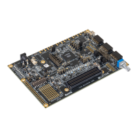
Figure A.7. Bank 3, 4, 5 I/O