Note 1: MAX2771 is production tested at T
A
= 25ºC. User must program the registers to the specified default settings upon
power-up.
Note 2: Default mode of the IC. PLL is an an integer-N mode with f
COMP
= f
TCXO
/16 = 1.023MHz and I
CP
= 0.5mA. The complex
IF filter is configured as a 5th-order Butterworth filter with a center frequency of 4MHz and bandwidth of 2.5MHz.
Output data is in a 2-bit sign/magnitude format at CMOS logic levels in the I channel only.
Note 3: The LNA output connects to the mixer input without a SAW filter between them.
Note 4: Two tones are located at 12MHz and 24MHz offset frequencies from the GPS center frequency of 1575.42MHz or
1227.6MHz depending on band. Passive pole at the mixer output is programmed to be 13MHz.
Note 5: Measured from the LNA input to the LNA output. Two tones are located at 12MHz and 24MHz offset frequencies from
the GPS center frequency of 1575.42MHz or 1227.6MHz depending on band.
Note 6: Same global conditions except tune LO to 1223.508 MHz which means change PLL integer divider ratio to 1196 and
program LOBAND bit to 1.
Note 7: Filter response measured with PGA gain setting of GAININ = 000100, and mixer pole set to 36 MHz (MIXPOLE = 1).
(MAX2771 EV kit, V
CC
= 2.7V to 3.3V, T
A
= -40°C to +85°C. Registers are set to the specified default states. LNA input is driven from
a 50Ω source. All RF measurements are done in the analog output mode with ADC bypassed. PGA gain is set to GAININ = 111010
through SPI interface, unless otherwise noted. Maximum IF output load is not to exceed 10kΩ||7.5pF on each pin. Typical values are
at V
CC
= 2.85V and T
A
= +25°C, unless otherwise noted. (Note 1))
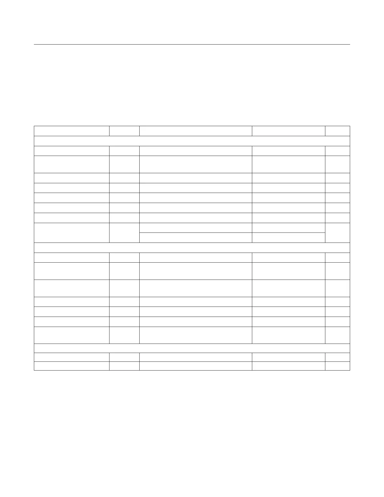
PARAMETER SYMBOL CONDITIONS MIN TYP MAX UNITS
AC ELECTRICAL CHARACTERISTICS/FREQUENCY SYNTHESIZER
LO Frequency Range 0.2V < V
TUNE
< (V
CC
- 0.25V), LOBAND = 0 1525 1610 MHz
LO Frequency Range—
L2/L5 Band
0.2V < V
TUNE
< (V
CC
- 0.25V), LOBAND = 1 1160 1290 MHz
LO Tuning Gain 70 MHz/V
LO Tuning Gain - L2/L5 Band 76 MHz/V
Reference Input Frequency 8 44 MHz
Main Divider Ratio 36 32,767 ─
Reference Divider Ratio 1 1023 ─
Charge-Pump Current
ICP = 0 0.5
mA
ICP = 1 1
AC ELECTRICAL CHARACTERISTICS/TXCO INPUT BUFFER/OUTPUT CLOCK BUFFER
Frequency Range Load = 10kΩ||10pF 8 44 MHz
Output High Level
With respect to ground, I
OH
= 10μA
(DC-coupled)
2 V
Output Low Level
With respect to ground, I
OL
= 10μA
(DC-coupled)
0.8 V
Capacitive Slew Current Load = 10KΩ||10pF, f
CLKOUT
= 44MHz 11 mA
Output Load 10||10 KΩ||pF
Reference Input Level Sine wave 0.5 V
P-P
Clock Output Multiply/
Divide Range
x2: max input frequency of 22MHz,
x4: max input frequency of 11MHz
/4 x4 ─
AC ELECTRICAL CHARACTERISTICS/ADC
ADC Dierential Nonlinearity AGC enabled, 3-bit output ±0.1 LSB
ADC Integral Nonlinearity AGC enabled, 3-bit output ±0.1 LSB
Electrical Characteristics (continued)
www.maximintegrated.com
Maxim Integrated
│
9
MAX2771 Multiband Universal GNSS Receiver