© 2009 MIMAKI ENGINEERING CO.,LTD.
2.3.5 P.1
1
2
3
4
5
6
7
8
R.1.0
Maintenance Manual > Electrical Parts > Circuit Board Specifications > Cutter Driver PCB Assy
Model CJV30/TPC Issued 2008.08.04 Revised F/W ver. 1.00 Remark
1.0
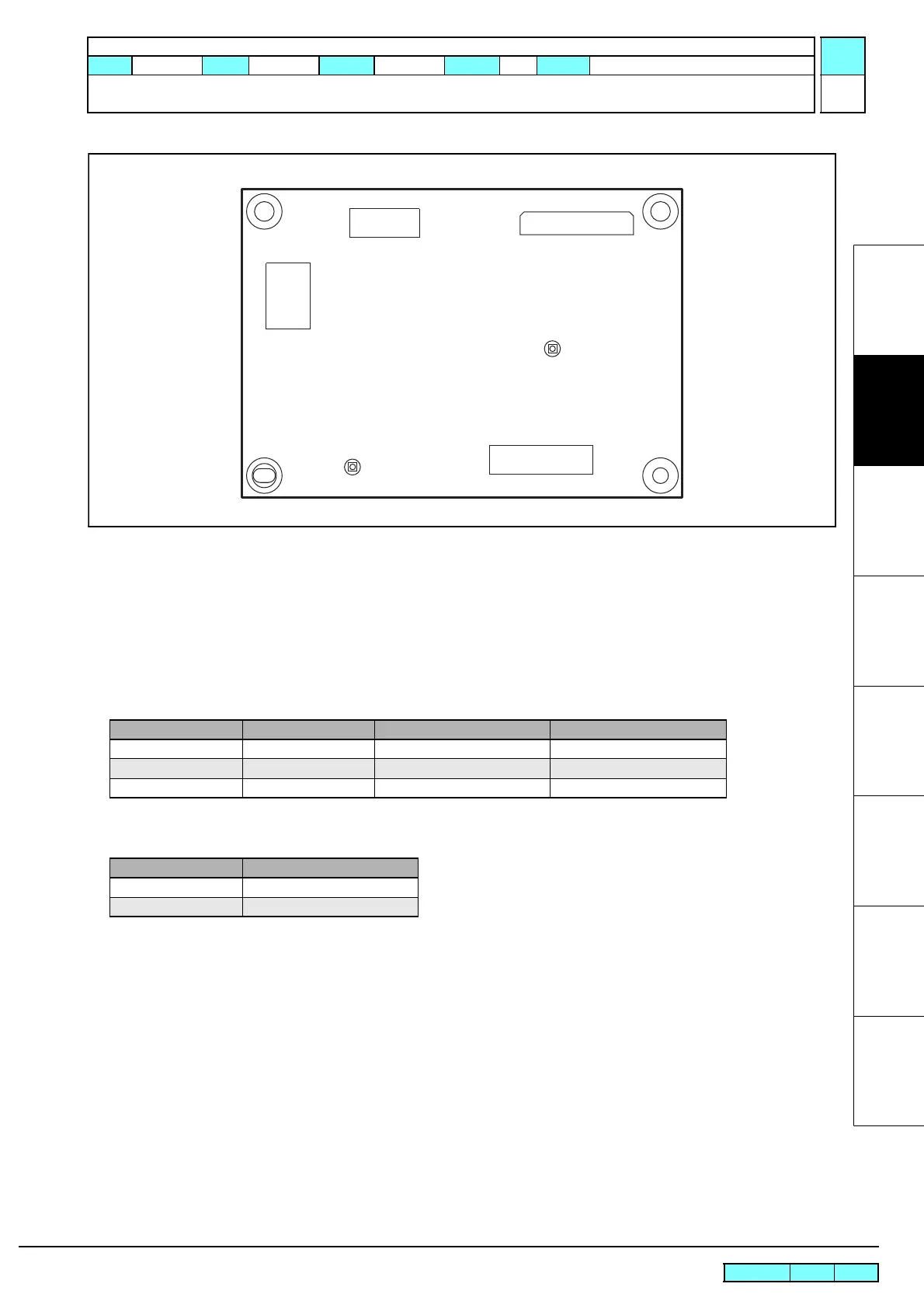
2.3.5 Cutter Driver PCB Assy
Outline
Board name: Cutter Driver PCB Assy
Is located on the main PCB assy inside the electrical box.
Controls I/O for the pen head, mark sensor and PR sensor.
List of connectors
Test poi nt
CN No Pin Connected to: Remarks
CN1 50 Main PCB Assy Control
CN2 8 Main PCB Assy Power source (for solenoids)
CN3 17 Cutter Slider PCB Assy Control / Power source
Terminal name Application
TP1 Output voltage of mark sensor
TPG1 GND
CN2
CN4
CN1
CN3
TP1
TPG1
 Loading...