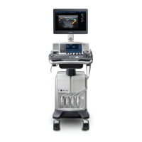
4-6 Product Principle
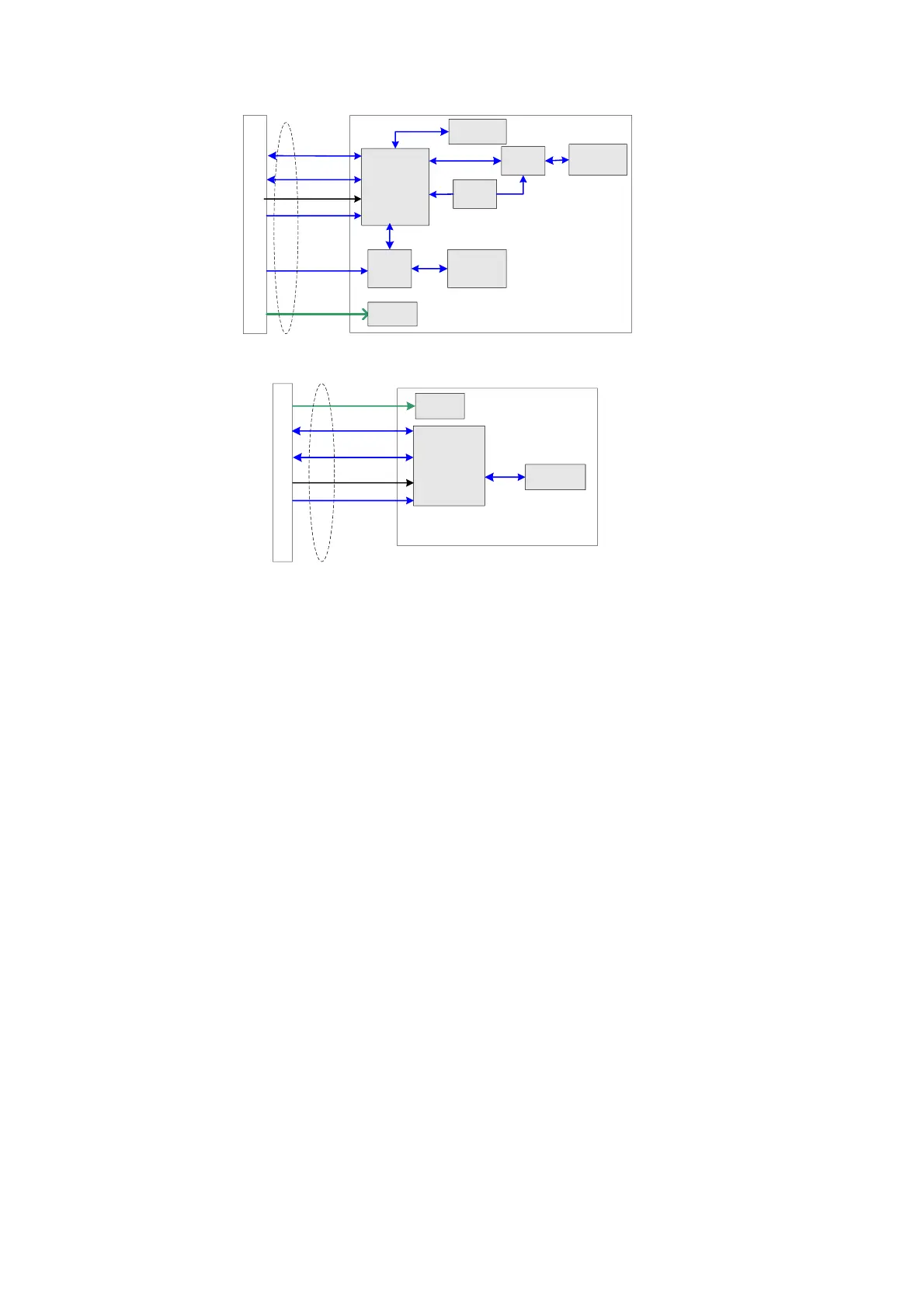
Communication motherboard
Signal
processing
FPGA
PCIe
Communic
ation bus
EDC+12V
Memory
Power
DSP
FPGA
SRIO
clock
Memory
Memory
Clock
Clock
Board-t-board connect socket
Data bus
Signal processing board
Fig 4-7 Schematic Diagram of Signal process board (support 4D and elastography)
Communication motherboard
Signal
processing
FPGA
PCIe
Communi
cation bus
EDC+12V
Memory
Power
Clock
Board-to-board connect socket
Data bus
Signal processing board
Fig 4-8 Schematic Diagram of Signal process board (not support 4D and elastography)
Function description:
Digital signal process in B, C, D imaging modes.
The imaging data will be packed and then uploaded to digital board CPU module for post
processing.
DSP chip is designed for elastography data processing, optional function.
A FPGA is designed for New Color etc. Signal processing, reserved function.
 Loading...