146
LCD PC E
LCD PC E
-
-
8590 MAINTENANCE
8590 MAINTENANCE
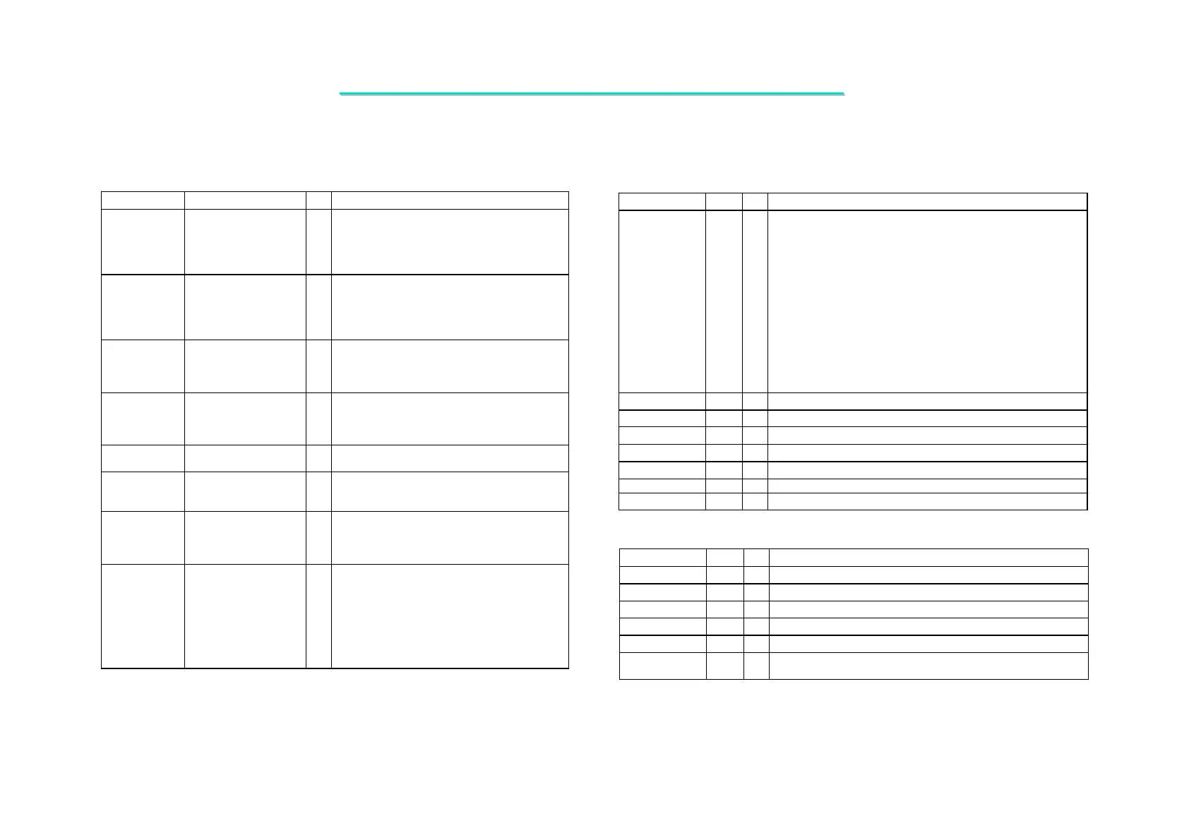
DRAM Interface continue
Signal Name Pin # I/O Signal Description
MAA[14:0]
AJ22, AE25, AG12, AJ7,
AH12, AF26, AG22,
AE22, AE20, AE21,
AF17,AG17, AJ17,AE16,
AF12
O
Memory Address A. DRAM address lines (two
sets for better drive). Output drive strength may be
set by Device 0 Rx6C[7-6].
MAB[14:0]
AG21, AE26, AJ11,
AH8,AE11, AF27, AE23,
AE24,AG19, AF21,
AJ18, AH17,AJ16,AG15,
AJ12
O
Memory Address B. DRAM address lines (two
sets for better drive). Output drive strength may be
set by Device 0 Rx6C[5-4].
SRASA#,
SCASA#,
SWEA#
AG16, AE10, AE14
O
Row Address, Column Address and Write
Enable Command Indicator Set A. (two sets for
better drive).Output drive strength may be set by
Device 0 Rx6C[7-6].
SRASB#,
SCASB#,
SWEB#
AD19, AD16, AD17
O
Row Address, Column Address and Write
Enable Command Indicator Set B. (two sets for
better drive).Output drive strength may be set by
Device 0 Rx6C[5-4].
CS[7:0]#
AE6, AE5, AF11, AE12,
AG7, AH6, AF8, AE9
O
Chip Select. Chip select of each bank. Output
drive strength may be set by Device 0 Rx6D[3-2].
DQM[8],
DQM[7:0] /
CKE[7:0]
AJ14,AD4, AJ1, AH5,
AJ9,AJ20, AJ24, AH27,
AE28
O
Data Mask. Data mask of each byte lane plus
DQM8 for ECC byte. Output drive strength may be
set by Device 0 Rx6D[5-4].
DQS[8],
DQS[7:0]# /
CKE[7:0]
AG14,AD3, AH1, AJ5,
AH9,AH20, AH24,
AJ28, AE29
IO
DDR Data Strobe. Data strobe of each byte lane
plus DQS8# for ECC byte. Output drive strength
may be set by Device 0 Rx6C[3-2].
CKE[7:0] /
MECC[7:0]
-or-
CKE[7:0] / D
QM[7:0]
-or-
CKE[7:0] / D
QS[7:0]#
O
Clock Enables. Clock enables for each DRAM
bank for powering down the SDRAM or clock
control for reducing power usage and for reducing
heat / temperature in high-speed memory systems.
See Device 0 Rx6B[4] for CKE function enable.
V-Link Interface
Signal Name Pin # I/O Signal Description
VAD7,
VAD6
/ strap
,
VAD5 / strap,
VAD4
/ strap,
VAD3 / strap,
VAD2
/ strap,
VAD1
/ strap,
VAD0 / strap
AB2
AB1
W2
AA5
W1
AB3
W3
W5
IO
IO
IO
IO
IO
IO
IO
IO
Address / Data Bus.
South Br.
Pin Strap Name Definition (L=strap low, H=high) Register Strap Pin
VAD6 Auto-Configure L=Disable (use on-chip defaults) Rx54[5]
SDA2H=Enable (get from ROMSIP)
VAD5 AGTL+ Drive Strength 4x L=1x, H=4x SDA1
VAD4 AGTL+ Drive Strength 2x L=1x, H=2x SDA0
VAD3 AGTL+ Internal Pullups L=Disable, H=Enable. Rx50[6] SA1
VAD2 In Order Queue Depth L=1-level, H=8-level. Rx50[7] SA18
VAD1 CPU Clock Speed Msb LL=66, LH=100, HL=Auto, Rx54[7]
SA17 VAD0 CPU Clock Speed Lsb HH=133 MHz Rx54[6] SA16
The above straps are not on the VADpi ns but on the indicated pin of
the south bridge chip.
The states of the south bridge strap pins are communicated to the
VT8703A via the VADpins.
VBE#
V5 IO
Byte Enable.
UPCMD
Y1 I
Command from Client-to-Host.
UPSTB
AA4 I
Strobe from Client-to-Host.
UPSTB#
Y3 I
Complement Strobe from Client-to-Host.
DNCMD
AA2 O
Command from Host-to-Client.
DNSTB
AA1 O
Strobe from Host-to-Client.
DNSTB#
AA3 O
Complement Strobe from Host-to-Client.
CRT Interface
Signal Name Pin # I/O Signal Description
AR
B6 AO
Analog Red.
Analog red output to the CRT monitor.
AB B5 AO
Analog Blue.
Analog blue output to the CRT monitor.
AG
A5 AO
Analog Green.
Analog green output to the CRT monitor.
HSYNC
B8 O
Horizontal Sync.
Output to CRT.
VSYNC
A8 O
Vertical Sync.
Output to CRT.
RSET
A6
AI
Reference Resistor.
Tie to GNDRGB through an external 140.
resistor to control the RAMDAC full-scale current value.
5.2 VIA VT8703 North Bridge with S3 Savage4 AGPX4