EasyManua.ls Logo

Mitsubishi MELSEC-Q/L User Manual

Mitsubishi MELSEC-Q/L
850 pages
To Next Page IconTo Next Page
To Previous Page IconTo Previous Page
Page #361 background imageLoading...
Page #361 background image
359
ENCO, ENCOP
1
2
3
4
4
6
7
8
7.5 Data processing instructions
7.5.4 ENCO, ENCOP
Program Example
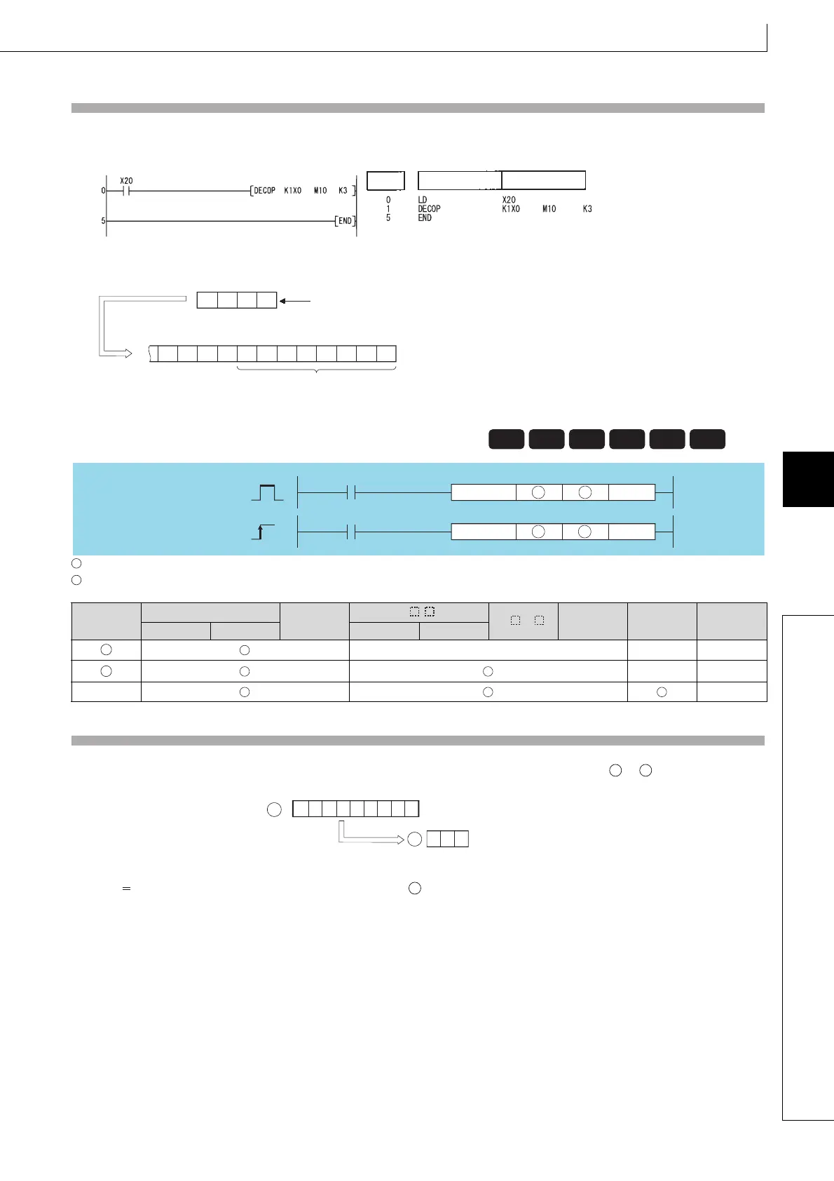
(1) The following program decodes the 3 bits from X0 and stores the results at M10 when X20 is ON.
[Ladder Mode] [List Mode]
[Operation]
: Head number of the device where the data to be encoded is stored (Device name)
: Number of the device where the encoding result will be stored (BIN 16 bits)
n : Valid bit length (1 to 8), 0: No processing (BIN 16 bits)
Function
(1) Stores the binary value corresponding to the bits which are "1" included in the 2
n
-bit data of to .
(2) The value of n can be designated at between 1 and 8.
(3) If n 0, there will be no operation, and the contents of will not change.
(4) Bit devices are treated as 1 bit, and word devices as 16 bits.
(5) If more than 1 bit is at 1, processing will be conducted at the upper bit location.
7.5.4 ENCO, ENCOP Encodi ng from 256 to 8 bits
7.5.4
ENCO, ENCOP
Setting
Data
Internal Devices
R, ZR
J\
U\G
Zn
Constants
K, H
Other
Bit Word Bit Word
–– –– ––
–– ––
n ––
Step
Instruction
Device
0 0 0 0 01 0 0 000
M10M17
0
If 3 bits are designated as significant bits, 8 points are occupied.
Decoding result
00
11
0
X0X1X2
When 6 is designated at X0 to X2
Basic
Process
High
performance
Redundant
Universal
LCPU
n
n
ENCO
ENCOP
D
D
Command
Command
ENCOP
ENCO S
S
S
D
S
D
S
D
7
0
86
(Binary value = 6)
543210
0 1000000
110
S
D
D

Table of Contents

Question and Answer IconNeed help?

Do you have a question about the Mitsubishi MELSEC-Q/L and is the answer not in the manual?

Mitsubishi MELSEC-Q/L Specifications

General IconGeneral
SeriesMELSEC-Q/L
TypeProgrammable Logic Controller
Input Voltage24V DC
I/O CapacityUp to 4096 I/O points
CommunicationEthernet, CC-Link, Serial (RS232, RS485), USB
Programming LanguageLadder Logic, Structured Text, Function Block Diagram, Instruction List, Sequential Function Chart
MemorySRAM, Flash Memory
Power Supply24V DC
Operating Temperature0 to 55°C
Storage Temperature-25 to 75°C
Humidity5% to 95% (non-condensing)
CPU TypeVarious models available (e.g., QCPU, LCPU)

Summary

SAFETY PRECAUTIONS

CONDITIONS OF USE FOR THE PRODUCT

REVISIONS

INTRODUCTION

CHAPTER 1 GENERAL DESCRIPTION

1.1 Related Programming Manuals

Lists other manuals required for understanding Q/L series CPU modules and their functions.

1.2 Abbreviations and Generic Names

Defines generic names and abbreviations used for Q/L series CPU modules.

CHAPTER 2 INSTRUCTION TABLES

2.1 Types of Instructions

Classifies CPU module instructions into major types like sequence, basic, application, data link, etc.

2.2 How to Read Instruction Tables

Explains the format and symbols used in instruction tables for understanding program logic.

2.3 Sequence Instructions

Details instructions related to sequence control, including contact, association, output, and shift operations.

2.4 Basic Instructions

Covers fundamental instructions like comparison, arithmetic, data transfer, and program control.

2.5 Application Instructions

Describes instructions for specific applications such as logical operations, rotation, bit processing, and data processing.

CHAPTER 3 CONFIGURATION OF INSTRUCTIONS

3.1 Configuration of Instructions

Explains the structure of CPU module instructions, consisting of instruction and device parts.

3.2 Designating Data

Details the six types of data that can be handled by CPU module instructions.

3.3 Indexing

Explains indexing as an indirect setting method for specifying devices using index registers.

CHAPTER 4 HOW TO READ INSTRUCTIONS

CHAPTER 5 SEQUENCE INSTRUCTIONS

5.1 Contact Instructions

Explains contact instructions like LD, LDI, AND, ANI, OR, ORI, and their connection types.

5.2 Association Instructions

Covers instructions for association like ANB, ORB, MPS, MRD, and MPP, used for memory storage and retrieval.

5.3 Output Instructions

Details output instructions like OUT, SET, RST, PLS, PLF, FF, DELTA, and DELTAP for controlling outputs.

5.4 Shift Instructions

Explains instructions for shifting data, including SFR, SFRP, SFL, and SFLP.

5.5 Master Control Instructions

Covers MC and MCR instructions for creating efficient ladder switching sequence programs.

5.6 Termination Instructions

Explains FEND and END instructions for program termination and sequence program end.

5.7 Other instructions

Lists other instructions like STOP, NOP, NOPLF, and PAGE, used for program control and stopping.

CHAPTER 6 BASIC INSTRUCTIONS

6.1 Comparison Operation Instructions

Explains instructions for comparing BIN 16-bit, BIN 32-bit, floating-point, and character string data.

6.2 Arithmetic Operation Instructions

Details arithmetic operations like addition, subtraction, multiplication, and division for BIN and floating-point data.

6.3 Data conversion instructions

Covers instructions for converting data between BCD, BIN, floating-point, and ASCII formats.

CHAPTER 7 APPLICATION INSTRUCTIONS

7.1 Logical operation instructions

Explains logical operations like AND, OR, XOR, and XNR for bit-wise data manipulation.

7.2 Rotation instruction

Covers instructions for rotating data bits, including ROR, ROL, DROR, and DRCL.

7.3 Shift instruction

Details shift instructions like SFR, SFRP, SFL, and SFLP for moving data bits.

7.4 Bit processing instructions

Explains instructions for bit manipulation such as BSET, BRST, TEST, and DTEST.

7.5 Data processing instructions

Covers instructions for data manipulation like search, sort, sum, average, decode, and encode.

7.6 Structure creation instructions

Explains instructions for creating program structures like FOR/NEXT loops, CALL, FCALL, ECALL, EFCALL, and XCALL.

7.7 Data Table Operation Instructions

Details instructions for managing data tables, including FIFW, FIFR, FPOP, FDEL, FINS.

7.8 Buffer memory access instruction

Covers instructions for accessing buffer memory, such as FROM, FROMP, DFRO, DFROP, TO, TOP, DTO, DTOP.

7.9 Display instructions

Explains instructions for displaying data, including PR, PRC, and LEDR.

7.10 Debugging and failure diagnosis instructions

Provides instructions for debugging and diagnosing failures, such as CHKST, CHK, CHKCIR, and CHKEND.

7.11 Character string processing instructions

Covers instructions for processing character strings, including BINDA, HABIN, DABCD, STR, EVAL, etc.

7.12 Special function instructions

Details special function instructions for mathematical operations like SIN, COS, TAN, ASIN, ACOS, ATAN, and their double precision counterparts.

7.13 Data Control Instructions

Explains instructions for data control, including LIMIT, BAND, and ZONE operations for range and dead band control.

7.14 File register switching instructions

Details instructions for switching file registers, such as RSET, QDRSET, QCDSET.

7.15 Clock instructions

Explains instructions for handling clock data, including DATERD, DATEWR, DATE+, DATE-, SECOND, HOUR, and TM instructions.

CHAPTER 8 INSTRUCTIONS FOR DATA LINK

8.1 Network refresh instructions

Covers instructions for refreshing network communication, specifically S.ZCOM and SP.ZCOM.

8.2 Reading/Writing Routing Information

Explains instructions for reading and writing routing information, like S.RTREAD, SP.RTREAD, S.RTWRITE, and SP.RTWRITE.

CHAPTER 9 MULTIPLE CPU DEDICATED INSTRUCTION

9.1 Writing to the CPU Shared Memory of Host CPU

Details instructions for writing data to the CPU shared memory, such as S.TO and TO.

9.2 Reading from the CPU Shared Memory of Another CPU

Explains instructions for reading data from the CPU shared memory of other CPUs, such as FROM, FROMP, DFRO, DFROP.

CHAPTER 10 MULTIPLE CPU HIGH-SPEED TRANSMISSION DEDICATED INSTRUCTIONS

10.1 Overview

Provides an overview of multiple CPU high-speed transmission dedicated instructions and their usage.

CHAPTER 11 REDUNDANT SYSTEM INSTRUCTIONS (For REDUNDANT CPU)

11.1 SP.CONTSW System Switching

Explains the SP.CONTSW instruction for switching between control and standby systems.

APPENDICES

Appendix 1 OPERATION PROCESSING TIME

Details the processing time for various instructions on different CPU modules.

Appendix 2 CPU PERFORMANCE COMPARISON

Compares the performance of QCPU, LCPU with AnNCPU, AnACPU, and AnUCPU.

Appendix 3 APPLICATION PROGRAM EXAMPLES

Provides example programs illustrating operations like nth power and nth root calculations.

WARRANTY

Related product manuals