574
DATEWR, DATEWRP
Function
(1) Writes clock data stored in the device number designated by or later device number to the clock element of the CPU
module.
(2) Each item is set as a BIN value.
(3) The "year" at is designated by using four-digit year indication between 1980 to 2079.
(4) +1 designates the "month" in values of from 1 to 12 (January to December).
(5) +2 designates the "day" in values of from 1 to 31.
(6) +3 designates the "hour" in values of from 0 to 23 (using 24-hour clock, from 0 hours to 23 hundred hours). (Uses the
24-hour clock.)
(7) +4 designates the "minute" in values of from 0 to 59.
(8) +5 designates the "second" in values of from 0 to 59.
(9) +6 designates the "day of week" in values of from 0 to 6 (Sunday to Saturday).
Operation Error
(1) In any of the following cases, an operation error occurs, the error flag (SM0) turns ON, and an error code is stored into
SD0.
Program Example
(1) The following program writes the following clock data to the clock element as BCD values when X40 is turned ON.
Year ..................X30 to X3F Hour......................... X18 to X1F
Month................X28 to X2F Minute...................... X10 to X17
Day ...................X20 to X27 Second..................... X8 to XF
Week ................X4 to X7
Day of week Sun Mon Tue Wed Thu Fri Sat
Stored data 0 1 2 3 4 5 6
Error
code
Error details
Q00J/
Q00/
Q01
QnH QnPH QnPRH QnU LCPU
4100 The value outside the setting range has been set for each item. –– –– –– ––
4101
The range of the device specified by exceeds the range of the
corresponding device.
–– –– –– ––
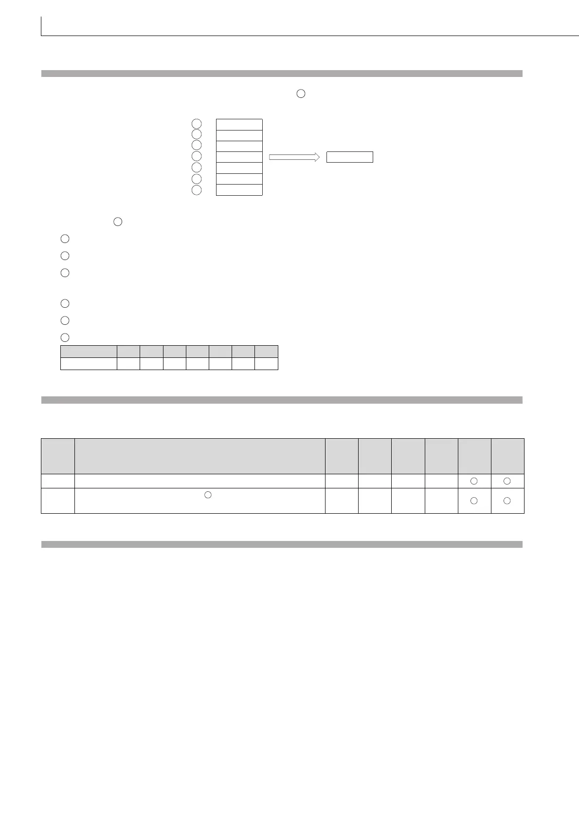
S
Year
Month
Day
+1
+2
+3
+4
+5
+6
Hour
Minute
Second
Day of week
Clock element
S
S
S
S
S
S
S
S
S
S
S
S
S
S
S
 Loading...