610
ZRWRB, ZRWRBP
Function
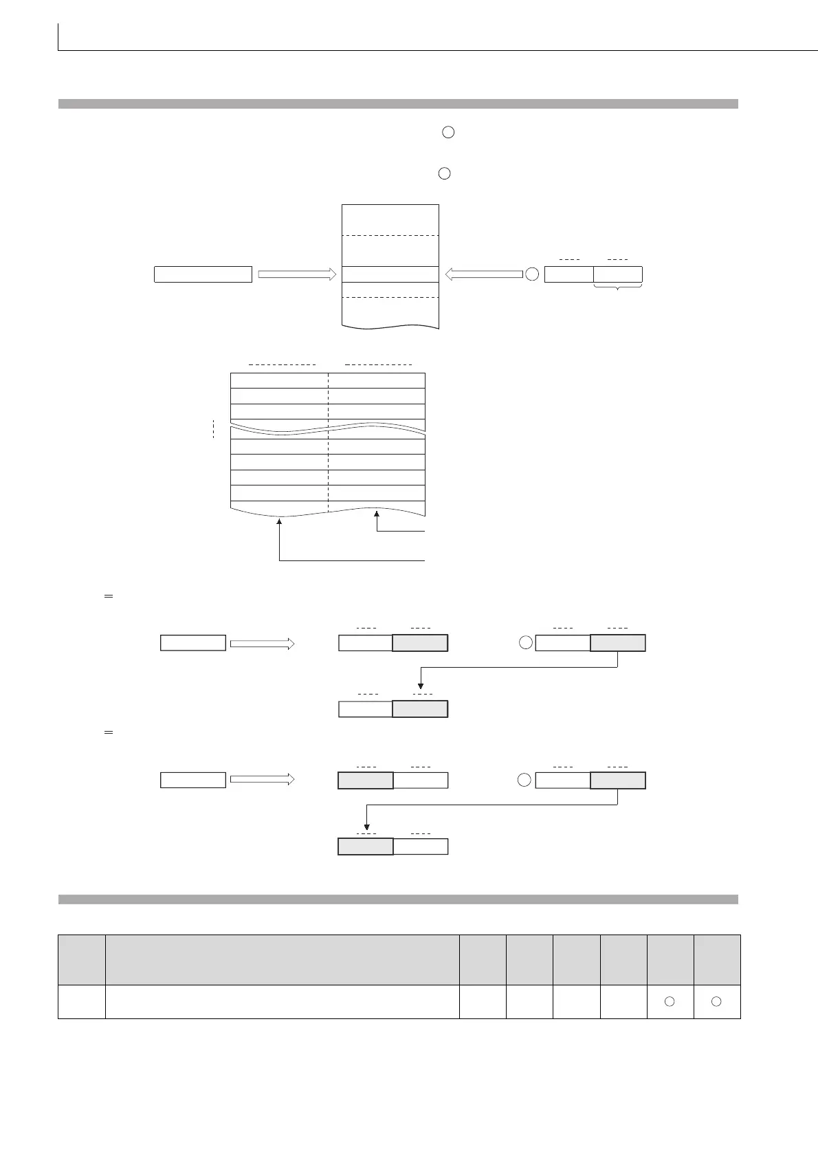
(1) Writes the lower 8 bits of data stored in the device designated by that does not signify a block number to the file
register of the serial byte number designated by n.
The upper 8 bits of data in the device designated by are ignored .
(2) The correspondence between file register numbers and serial byte numbers is as indicated below:
If n 12340 is specified, the data will be written to the lower 8 bits of ZR6170.
If n 43257 is specified, the data will be written to the upper 8 bits of ZR21628.
Operation Error
(1) In the following case, an operation error occurs, the error flag (SM0) turns ON, and an error code is stored into SD0.
Error
code
Error details
Q00J/
Q00/
Q01
QnH QnPH QnPRH QnU LCPU
4101
The specified device number (serial byte number) exceeds the
available range.
–– –– –– ––
S
S
Area for
block No. 0
Area for
block No. 1
Area for
block No. 2
ZR65536
ZR65535
ZR32768
ZR0
ZR32767
Serial byte number
n
Contents to
be written
Ignored
b0b7b15 b8
Write destination
designation
Writing the data
File register
S
ZR0
Serial byte No. 0Serial byte No. 1
Serial byte No. 2Serial byte No. 3
ZR1
Serial byte No. 4
Serial byte No. 5
Serial byte No. 5000Serial byte No. 5001
Serial byte No. 5002Serial byte No. 5003
Serial byte No. 5004Serial byte No. 5005
Serial byte No. 5006
Serial byte No. 5007
ZR2501
ZR2502
ZR2503
Storage destination
when an even number is designated
Storage destination
when an odd number is designated
ZR2
ZR2500
b15 b8
b7
b0
b15 b8
b7
b0
ZR6170
43
H
b15 b8
b7
b0
Ignored
Write destination
designation
n
12340
b15 b8b7 b0
43
H
S
21
54
54
H
H
H
b15 b8 b7 b0
ZR21628
50
H
b15 b8 b7 b0
Ignored
Write destination
designation
n
43257
b15 b8 b7 b0
50
H
S
43
H
12
H
43
H
 Loading...