N10_Hardware_User_Guide
Copyright © Neoway Technology Co., Ltd.
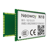
Figure 3-23 Reference design for speaker output
SPK@8Ω
GPRS module
33 pF
33 pF
100 pF
SPK_N
SPK_P
3.8 RF
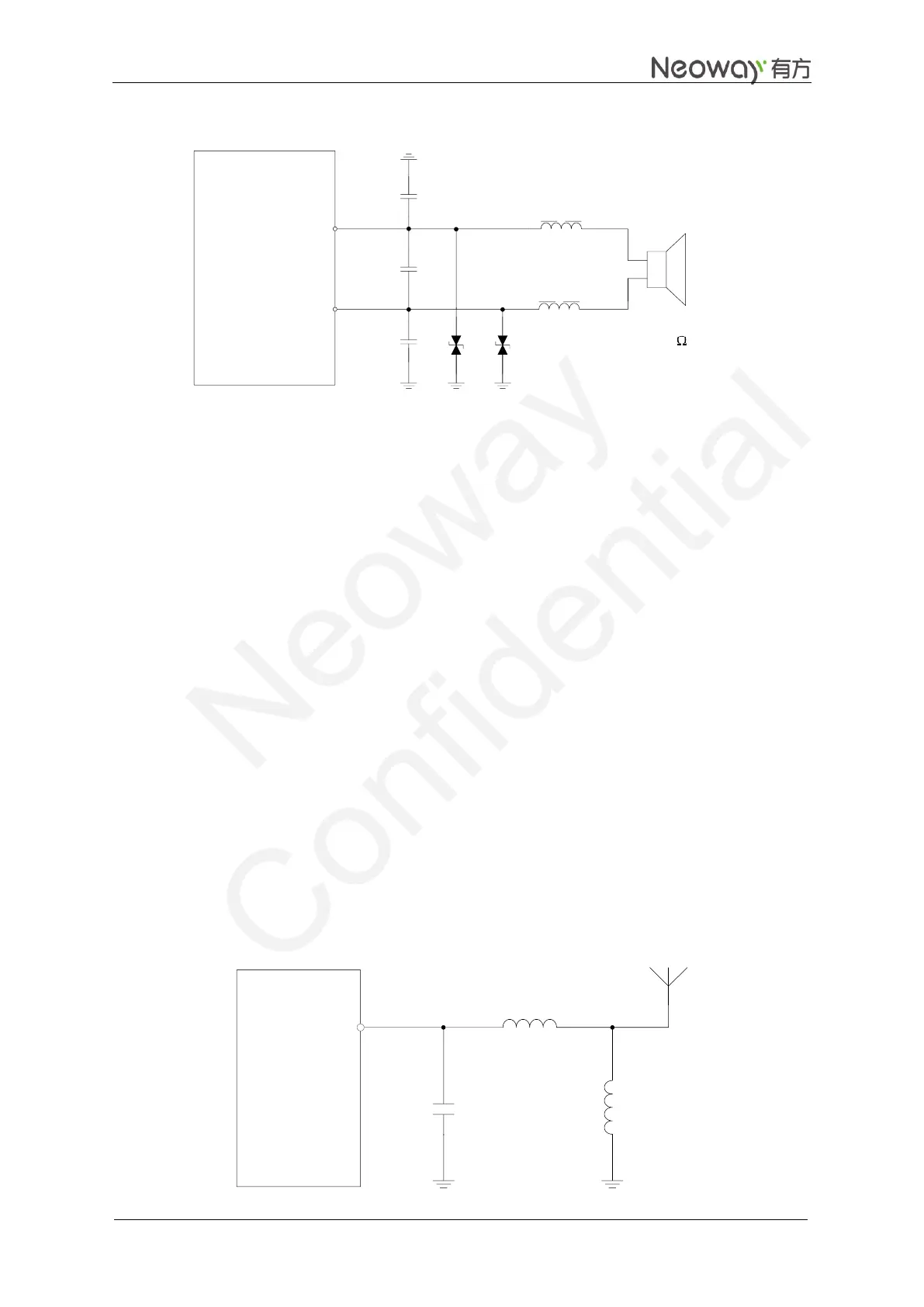
3.8.1 RF Design and PCB Layout
A 50 Ω antenna is required. VSWR ranges from 1.1 to 1.5. The antenna should be well matched to
achieve best performance. It should be installed far away from high speed logic circuits, DC/DC power, or
any other strong disturbing sources.
For multi-layer PCB, the trace between the antenna pad of module and the antenna connector, should have
50 Ω characteristic impedance, and be as short as possible. The trace should be surrounded by ground
copper. Place plenty of via holes to connect this ground copper to main ground plane, at the copper edge.
If the trace between the module and connector has to be longer, or built-in antenna is used, a π-type
matching circuit should be needed, as shown in Figure 3-24. The types and values of C1, L1, and L2
should be verified by using network analyzer instrument. If the characteristic impedance is well matched,
and VSWR requirement is met, just use a 100 pF capacitor for C1 and leave L1, L2 un-installed.
Avoid any other traces crossing the antenna trace on neighboring layer.
Figure 3-24 Reference design for antenna interface
GPRS
Module
ANT
C1
GPRS_ANT
L2
L1