N10_Hardware_User_Guide
Copyright © Neoway Technology Co., Ltd.
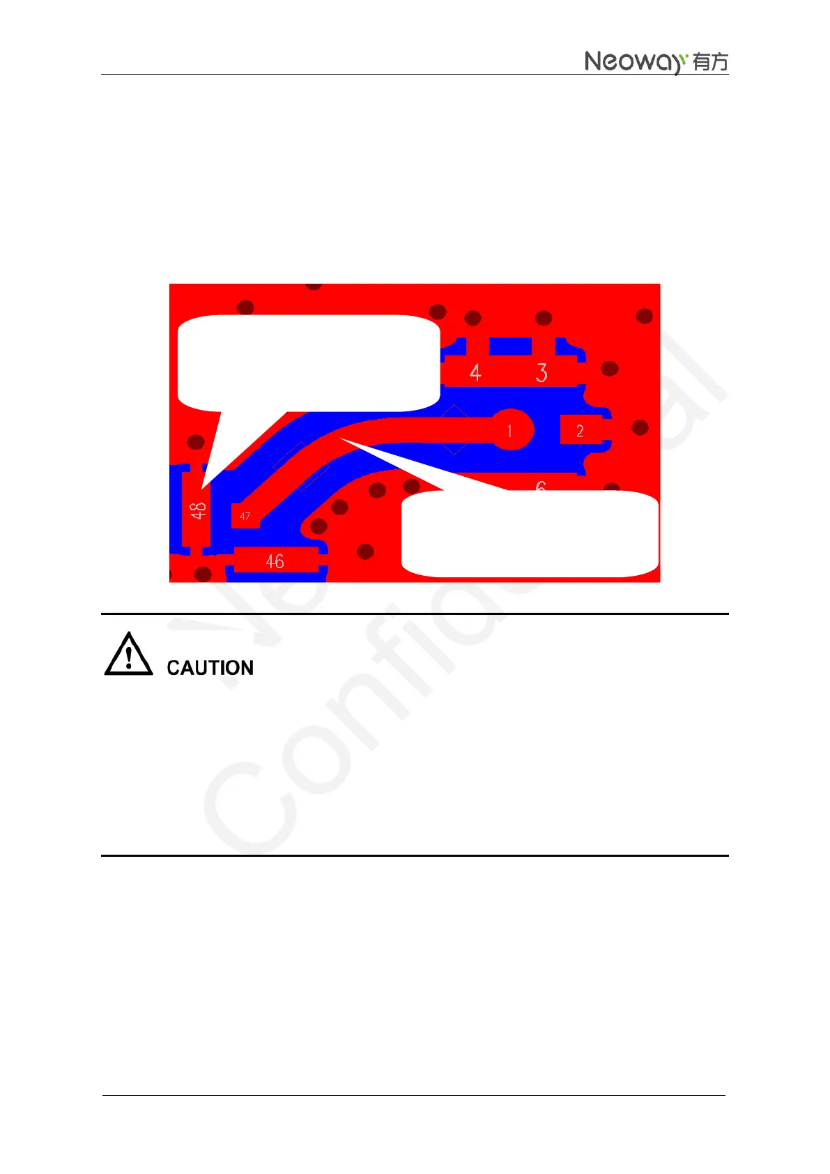
On two-layer boards which cannot control resistance properly, the RF route should be as short and
smooth as possible and at a width of 0.5 mm; the RF is 0.5 mm away from the ground.
Figure 3-25 shows a two-layer board application. The RF is connected to GSC RF connector through
traces on PCB, which is connected to the antenna via cable.
Figure 3-25 RF layout reference
ESD protection is built in module. For special ESD protection, an ESD diode can be placed close to the
antenna. But ensure using a low junction capacitance ESD diode. The junction capacitance should be less
than 0.5 pF, otherwise the RF signal will be attenuated. RCLAMP0521P from Semtech, or ESD5V3U1U
from Infineon, can be used here.
On the PCB, keep the RF signals and RF components away from high-speed circuits, power supplies,
transformers, great inductors, the clock circuit of single-chip host, etc.
3.8.2 Recommended RF Connection
If RF cables are used for connections, the GSC RF connector MM9329-2700RA1 from Murata is
recommended. Figure 3-26 shows the encapsulation specifications.
The RF traces are wide 0.5 mm; leave
space at least 0.5 mm between the
coppers. Drill enough grounding holes.
Ensure that the ground pins on both
sides of the antenna are grounded
completely and they form a complete
circle with grounding copper.