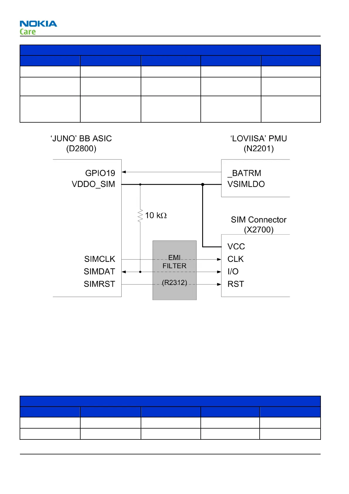
SIM Interface
Pin Name Pin I/O Type Description
SIMDAT D12 I/O CMOS SIM data signal
GPIO19 V6 I CMOS SIM emergency
shut-down
SIMVDDO A12 1.8V / 3.0V Digital
Supply for SIM
Transceivers
Figure 44 Electrical interface between baseband and SIM
Electrical Interface Between Baseband and Memory Card
Introduction
The D2800 JUNO (BCM21351) BB ASIC has an integrated SDIO interface which can be used to support an
external memory card. The SDIO interface I/O buffers are protected by the Z2301 EMI filter. In addition to the
integrated SDIO interface, GPIO15 is used as a card detection signal from the uSD card slot.
The signals on the SDIO interface can support 1.8V or 3.0V CMOS signaling levels. The VHCLDO2 supply from
the N2201 LOVIISA PMU determines the signaling levels.
Table 14 D2800 Baseband ASIC (BCM21351) Memory Card Interface Pins
SDIO #1
Pin Name Pin I/O Type Description
SD1CK F14 O CMOS SDIO Clock
SD1CMD B13 I/O CMOS SDIO Command
RM-497
System Module
Page 5 – 30 COMPANY CONFIDENTIAL Issue 1
Copyright © 2010 Nokia. All rights reserved.