Pin Name Pin I/O Type Description
LCDD1 F11
LCDD2 A10
LCDD3 B10
LCDD4 D10
LCDD5 B9
LCDD6 E10
LCDD7 D9
GPIO24 A11 O CMOS LCD Reset
GPIO25 B11 I CMOS LCD Panel Tearing Effect
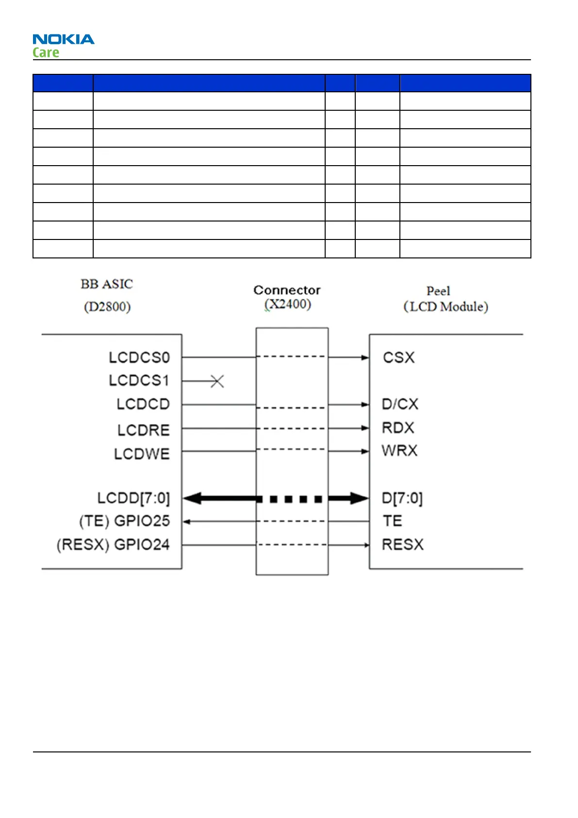
Figure 46 D2800 Baseband ASIC (BCM21351) Display Interface Pins
Electrical Interface Between Baseband and Keypad
Introduction
The D2800 JUNO (BCM21351) BB ASIC uses it’s GPIOs for the keypad interface. The keypad interface orients
the keys in rows and columns where GPIO[0:5] are used for rows 0 through 5 and GPIO[8:11] are used for
columns 0 through 3. The keypad is on a seperate PWB connected to the mainboard by connector X2420.
The GPIO I/O buffers on the D2800 JUNO are protected by the Z2400 EMI filter.
All GPIOs use 1.8V CMOS signaling levels.
RM-497
System Module
Page 5 – 32 COMPANY CONFIDENTIAL Issue 1
Copyright © 2010 Nokia. All rights reserved.