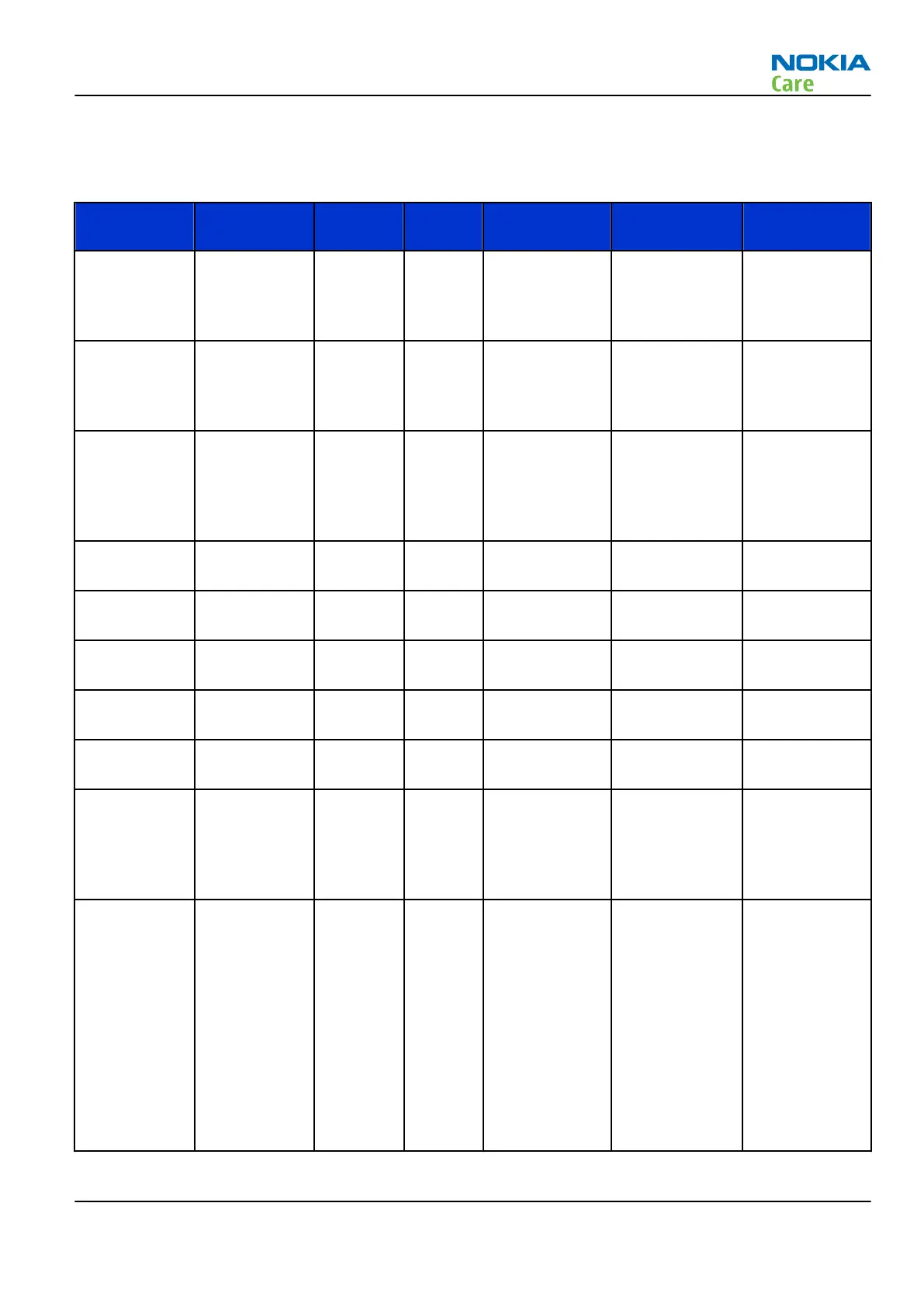
General power checking
Check the following supply voltages from the N2201 Loviisa PMU to the D2800 Juno BB ASIC:
Signal name Regulator Sleep Active Main user Probe point Nominal
voltage (V)
VUSB2 VMSLDO2 ON ON NVM digital
supply, analog
supply for USB
I/O
C2219 3.3
VIO VIOLDO ON ON CMOS I/O
digital supply,
digital supply
for BBL I/O
C2222 1.8
VCORE VCSRL ON ON core digital
supply, digital
supply for RF,
analog supply
for USB PLL
C2200 1.2/1.01
VRF2 VRFLDO1 OFF ON analog supply
for RF
C2214 2.7
VRF1 VLVLDO2 OFF ON analog supply
for RF
C2209 1.3
VDCXO VLCLDO OFF ON analog supply
for RF
C2212 1.3
VSIM VSIMLDO TBD ON digital supply
for SIM I/O
C2215 3.0
VAMP2 VHCLDO2 OFF ON digital supply
for SDIO I/O
C2216 1.8
VMEM VIOSRL ON ON digital supply
for nvSRAM I/
O, digital
supply for EMI
I/O
C2201 1.8
VANA1 VLVLDO1 ON ON analog supply
for MainPLL,
analog supply
for AppsPLL,
analog supply
for USB,
analog supply
for USB, CSI-2/
CCP2 I/O, DSI I/
O, analog
supply for dual
DAC
C2208 1.2
RM-497
BB Troubleshooting and Manual Tuning Guide
Issue 1 COMPANY CONFIDENTIAL Page 3 – 9
Copyright © 2010 Nokia. All rights reserved.