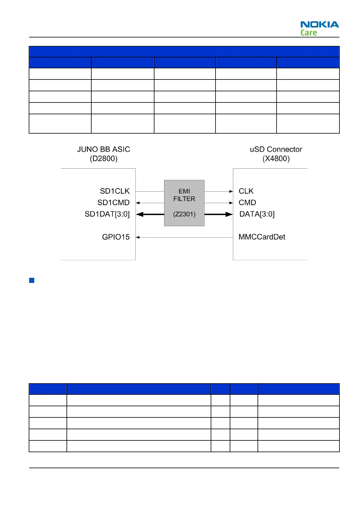
SDIO #1
Pin Name Pin I/O Type Description
SD1DAT0 E14 I/O CMOS SDIO Data bus
SD1DAT1 D13
SD1DAT2 A14
SD1DAT3 E13
GPIO15 U5 I CMOS Card Detect/
Hotswap
Figure 45 Electrical interface between baseband and memory card
User interface
Electrical Interface Between Baseband and Displays
Introduction
The D2800 (BCM21351) BB ASIC drives the LCD panel. The LCD panel uses 8-bit Messi (DBI-B) signaling.
Additionally, GPIO25 is used as a tearing effect signal from the LCD panel and GPIO24 is used as a single reset
signal.
The LCD signals are connected to LCD panel through the X2400 Connector.
All signals on the LCD interface use 1.8V CMOS signaling levels.
D2800 Baseband ASIC (BCM21351) Display Interface Pins
Pin Name Pin I/O Type Description
LCDCS0 B8 O CMOS LCD Panel chip select
LCDCD D11 O CMOS LCD command/data select
LCDWE E8 O CMOS LCD write enable
LCDRE E9 O CMOS LCD read enable
LCDD0 E11 I/O CMOS LCD 8-bit data bus
RM-497
System Module
Issue 1 COMPANY CONFIDENTIAL Page 5 – 31
Copyright © 2010 Nokia. All rights reserved.