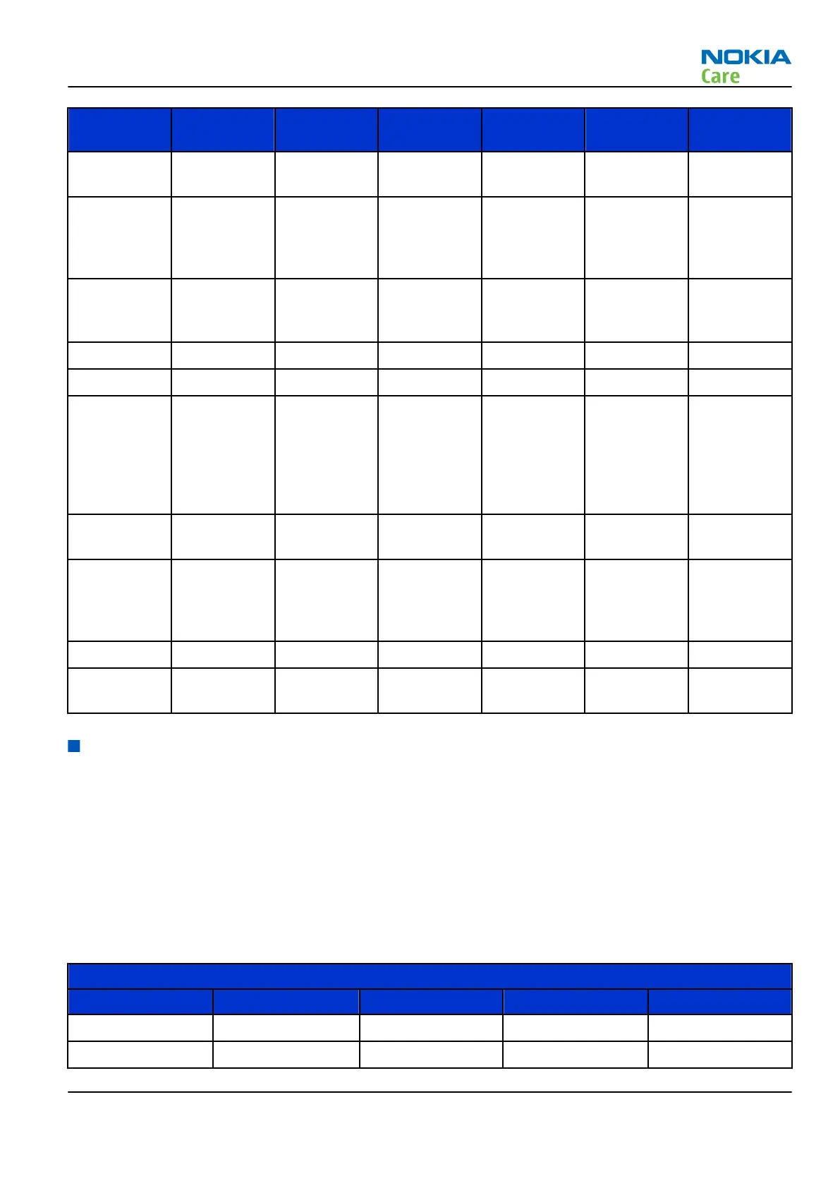
Signal Name Regulator
Type
PMU Pin Status on
reset
Rating (V) Rated (mA) 21351
Function
VANA2 LDO ALDO2 ON 2.5 150 Analog:ADC
(1-4) & IHF
VANA3 LDO ALDO1 ON 3 150 Analog:
u_phone,au
x ADC/DAC,
Dual DAC
VCORE SR CSR ON 1.2 500 Vcore
Digital, USB
PLL, RF_DSP
VDCXO LDO LCLDO ON 1.3 20 RF_DCXO
VIO LDO IOLDO ON 1.8 200 BBL, IO
VMEM SR IOSR ON 1.8 500 Flash & DDR
Memories,
External
Memory
interface,
NVRAM
VOUT LDO RFLDO2 ON 2.5 150 Analog:
USB , ACI
VRF1 LDO LVLDO2 OFF 1.3 150 RF: RX, PLL,
IF,
TX_PLL,TX_L
O
VRF2 LDO RFLDO1 OFF 2.7 150 RF: PA , RX
VUSB2 LDO MSLDO2 ON 3.3 150 USB: Analog,
NVM
SIM, µSD
Electrical Interface Between Baseband and SIM
Introduction
The SIM interface on the D2800 JUNO (BCM21351) BB ASIC works in conjunction with the N2201 LOVIISA PMU
to support emergency shut-down. When the PMU detects that the battery has been removed, it will notify
the D2800 JUNO BB ASIC which will then start an orderly shutdown of the SIMCLK, SIMRST, and SIMDAT pins.
The PMU will then disable the VSIMLDO supply.
The signals on the SIM interface can support 1.8V or 3.0V CMOS signaling levels. The VSIMLDO supply from the
N2201 LOVIISA PMU determines the signaling levels.
SIM Interface
Pin Name Pin I/O Type Description
SIMCLK B12 O CMOS SIM clock
SIMRST E12 O CMOS SIM reset signal
RM-497
System Module
Issue 1 COMPANY CONFIDENTIAL Page 5 – 29
Copyright © 2010 Nokia. All rights reserved.