Table 3 FEM Supplies/Control Signals
# Signal Name Test Point Voltage (All Bands)
1 VBAT (FEM Supply) C7529 3.7V
2 TX_EN C7525 1.8V
3 TR_SW_EN C7521 1.8V
4 MODE C7522 1.8V
5 BS1 C7523 1.8V
6 BS2 C7524 1.8V
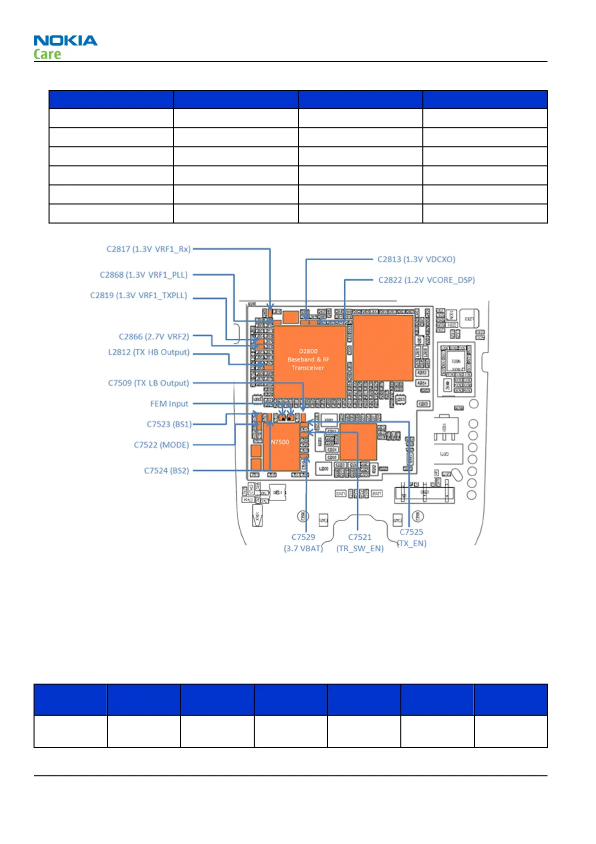
Figure 24 General voltage checking test points (main board, bottom side)
FEM Control Signal
When troubleshooting the FEM, it’s important to check its’ control signal. If the control signal didn’t operate
correctly, FEM might not turn on or it might turn on in different mode. Table xxx shows the control logic for
TX_EN, BS1, BS1, MODE, and TX_SW_EN. Figure xxx shows the timing diagram that one expects when probing
these signals.
Table 4 FEM Control Logics
Operational
State
TX_EN BS1 BS2 MODE TX_SW_EN Notes
Sleep/
standby
0 0 0 0 0
RM-497
RF troubleshooting
Page 4 – 8 COMPANY CONFIDENTIAL Issue 1
Copyright © 2010 Nokia. All rights reserved.