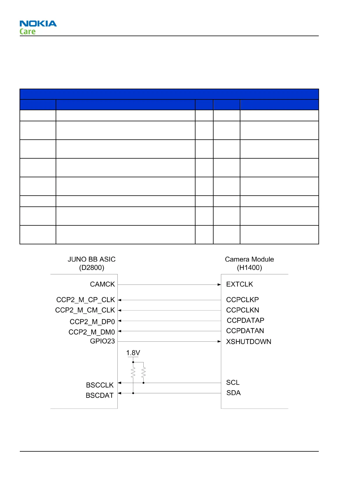
The CAMCK and GPIO23 signals use 1.8V CMOS signaling levels. The BSC (I2C-compatible) interface open-drain
I/O are also referenced to 1.8V. The differential clock and data signals from the camera use 1.2V CCP-2 (LVDS)
signaling levels.
D2800 Baseband ASIC (BCM21351) Camera Interface Pins
CCP-2 Serial Camera Interface
Pin Name Pin I/O Type Description
CAMCK W5 O CMOS Clock to camera
CCP2_M_C
P_CLK
AC6 I CCP-2 CCP-2 Differential Clock
CCP2_M_C
M_CLK
AC5
CCP2_M_D
P0
AB6 I CCP-2 CCP-2 Differential Data
CCP2_M_D
M0
AB5
GPIO23 V10 O CMOS Shutdown
BSCCLK W4 O Open-
Drain
BSC #2 (I2C-compatible)
clock
BSCDAT Y4 I/O Open-
Drain
BSC #2 (I2C-compatible)
data
Figure 49 D2800 baseband ASIC (BCM21351) camera interface pins
RM-497
System Module
Page 5 – 36 COMPANY CONFIDENTIAL Issue 1
Copyright © 2010 Nokia. All rights reserved.