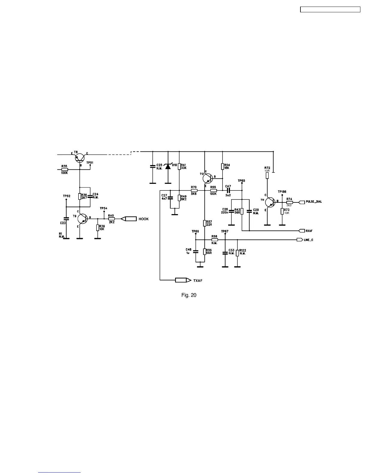
5.2.5. HOOKSWITCH (SEE Fig. 20)
T8 is the hookswitch, driven by T9. When the phone is “off-hook”, the HOOK control signal from the BBIC will be a high logic level
(+3V), and both transistors will be on, thus T8 will “loop” the line. The zenner diode D10 protects transistors T11 to T13 against
transient line voltages.
5.2.6. PULSE DIALING (SEE Fig. 20)
During pulse dialing the hookswitch (T8, T9) is used to generate the pulses using the HOOK control signal, which is set high
during pulses. To force the line impedance low during the “pause” intervals between dial pulses, the PULSE-DIAL signal turns
on T11.
5.2.7. AUDIO CIRCUITS (SEE Fig. 20)
The line output signal from the BBIC RXAF is amplified by T13. The RXAF line is DC coupled to T13 thus making it work as
a current limiter (typically < 8mA). The emitter load of T13 is complex to achieved the correct frequency response, since the line
load is also complex.
The line input signal TXAF is taken from the junction of R41 and R70.
Phase cancellation of the line output audio occurs at this point, so that only incoming line audio should be passed to the BBIC
on TXAF.
Circuit Diagram
21
KX-TCD705RUM / KX-TCD705RUS
 Loading...