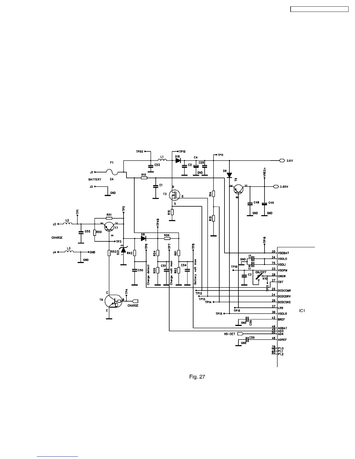
6.1.11. BATTERY SUPPLY (SEE Fig. 27)
A switch mode boost converter is used to provide a 3.8V supply from the battery. This supply is sensed by the BBIC through
pin 26 (TP14) so that the switching rate can be controlled by a FET (T3) driven from pin 24 (TP13). A resistor on the Source
of the FET provides a current sense at pin 25 (TP12).
T3 switches the current through L1. When T3 switches off the back emf conducts through D16 and charges the reservoir cap
C4.
6.1.12. 2.65V REGULATOR (SEE Fig. 27)
A 2.65V supply is provided for the BBIC and is regulated by the BBIC’s on board control signal LRB (pin 37).
This reference is fed to the base of T6 to keep the “VREG+” line at 2.65V.
6.1.13. BATTERY CHARGING CIRCUIT (SEE Fig. 27)
The supply for the battery comes from the charge terminals at J3 and J4. Battery charge rate is controlled by switching the
current through T7 such that the average charging current is 170mA. The current flow is monitored at pin 49 of the BBIC by
measuring the voltage across R56.
D21 protects against the high voltage present on the charge contacts (J3 and J4) when there is no battery in the handset. R42
and C50 provide a signal to the BBIC (pin 27) to detect that the handset has been placed on the base charger.
Circuit Diagram
29
KX-TCD705RUM / KX-TCD705RUS