VMP2 Preface
ID 24855, Rev. 02 Page 0 - 11© 2002 PEP Modular Computers GmbH
List of Figures
2-1 Functional Block Diagram............................................................................2 - 3
2-2 Front Panels ................................................................................................ 2 - 4
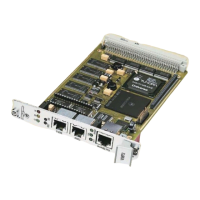
2-3 VMP2 Board (Front View)............................................................................2 - 5
2-4 VMP2 Board (Reverse View)....................................................................... 2 - 5
2-5 VME Connector CON1 ................................................................................ 2 - 9
2-6 Ethernet Connector CON8 ........................................................................ 2 - 11
2-7 Serial Port Connectors CON6 and CON7 ................................................. 2 - 12
2-8 PCI Expansion Connector CON11.............................................................2 - 13
2-9 Memory Expansion Connector IC8............................................................2 - 16
2-10 DEBUG Connector CON10 .......................................................................2 - 17
4-1 VMP2 Address Map..................................................................................... 4 - 7
4-2 VME Address Area ..................................................................................... 4 - 8
4-3 VMP2 Device Address Map.........................................................................4 - 9
A-1 Board Layout (Front View)...........................................................................A - 5
A-2 VMP1-IO1 Front Panel ................................................................................A - 6
A-3 Installation Diagrams...................................................................................A - 9
B-1 Plan and Profile Views of VMP1-Post Module.............................................B - 4
C-1 View of underside of RS485 Module ...........................................................C - 3
D-1 JTAG Chain Illustration................................................................................D - 3
D-2 Resistor Positions on Reverse of VMP2 Board ..........................................D - 4
E-1 View of Underside of the CP320-TR1 Module.............................................E - 3
F-1 View of Underside of CP320-TR2 Module...................................................F - 4
G-1 PMC-HDD1 Module with Hard Disk Drive Attached ................................... G - 3