4-10 888-2408-002
WARNING: Disconnect primary power prior to servicing.
Overall System Theory
4.3.4.3 PA Modules
Each of the 8 PA Modules contain two PA Amplifier boards mounted on opposite
sides of the PA Module heat sink. The modules are numbered 1 through 8 with the
top module in the front being #1 and counting to #4 at the bottom. The top rear
module is #5 counting down to #8 at the bottom rear, see Figure 4-5 for the front
view and Figure 4-6 for the rear view. The PAs are numbered as 1A, 1B, 8A, 8B
etc... with the “A” side PAs being plugged into the “A” Z Plane, and the “B” PAs
plugged into the “B” Z Plane. From the front of the transmitter, the “A” Z Plane is
on the right and the “B” Z Plane is on the left. Keep in mind this is reversed when
viewing from the rear of the transmitter. All DC, signal and RF connections to a PA
board are through one edge connector.
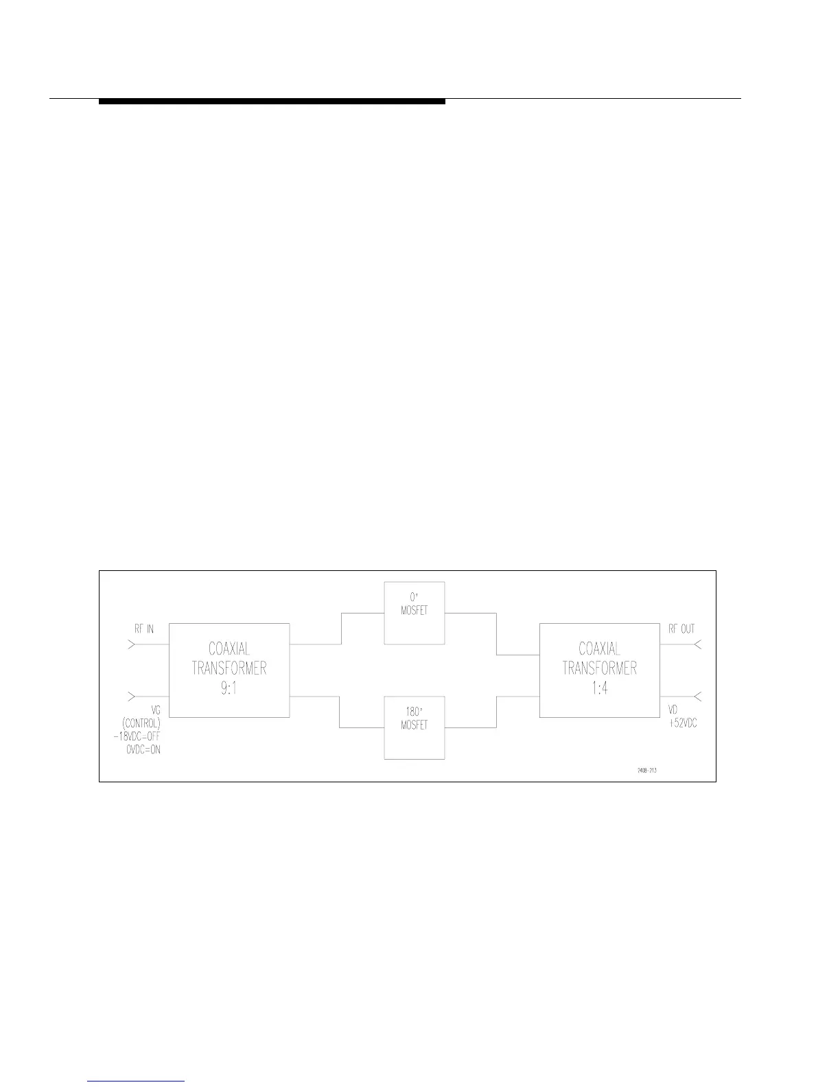
4.3.4.4 Power Amplifier (PA)
See Figure 4-4. The RF drive from the IPA enters the PA Amplifier Boards at Pin C.
The RF input level for each amplifier is typically 15-20 watts. TL1, C1 and C2
allow the input impedance to be matched to 50 ohms and permit the phase shift
through the module to be trimmed to a nominal value which allows all modules to
combine in-phase. The RF signal is then sent to T1, a coaxial 9:1 transformer which
also splits the phase providing 0 degree and 180 degree outputs to drive a pair of
push-pull RF power MOSFETs (Q1 and Q2). Bias to Q1 and Q2 (labeled VG for
Gate Voltage) is connected through the center of the secondary winding of T1.
Figure 4-4 Power Amplifier Block Diagram
The control voltage input called VG can be thought of as a bias voltage which can
be used to vary the amplifier output. Normally for the PAs it is simply used to turn
the amplifiers on and off. If VG is -18V the amplifier is off or muted. If VG is 0V
the amplifier is fully turned on and drive level from the IPA determines the
amplifier power output.