EasyManuals Logo

Renesas RH850 User Manual

Renesas RH850
67 pages
To Next Page IconTo Next Page
To Previous Page IconTo Previous Page
Page #11 background imageLoading...
Page #11 background image
RH850/U2A 292pin 1. Overview
R20UT4970ED0101 Rev.1.01 Page 11 of 67
July 08, 2022
1.6 Modifications for U2A6 device
In order to use a U2A6 device with this piggyback board it is necessary to modify the board.
Following connections must be changed:
Device
Ball
U2A16/8
U2A/6
Item to be
modified
J17
RX_DATA_P
VSS
RB2
K17
RX_DATA_N
VSS
RB1
H16
TX_DATA_P
E0VCC
RB3
J16
TX_DATA_N
E0VCC
RB3
K16
GETH0BVCC
E0VCC
JP2
G17
GETH0PVCC
E0VCC
JP3
H17
GETH0RVCC
E0VCC
JP22
E17
GETH0VCL
VSS
RB5
The jumpers JP2, JP3 and JP22 must have the same setting as JP6 (E0VCC).
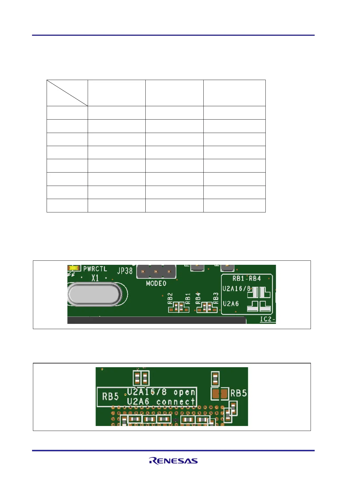
The four 0R resistors RB1-RB4 are on the upper side of the pcb. The setting of RB1-RB4 for
U2A16/8 or U2A6 use is printed on the pcb (Fig. 1.6).
On the lower side of the pcb there is preparation to add a solder bridge for the connection of
RB5.
Figure
1.6 RB1-RB4 setting
Figure
1.7 RB5 setting

Table of Contents

Questions and Answers:

Question and Answer IconNeed help?

Do you have a question about the Renesas RH850 and is the answer not in the manual?

Renesas RH850 Specifications

General IconGeneral
Memory ProtectionYes
CPU CoresSingle, Dual
PackageLQFP, BGA
Target ApplicationsAutomotive, Industrial
Functional SafetyISO 26262 ASIL-D compliant
Communication InterfacesCAN, Ethernet, SPI, I2C, UART

Related product manuals