RH850/U2A 292pin 3. Power Supply
R20UT4970ED0101 Rev.1.01 Page 22 of 67
July 08, 2022
3.2 Voltage Distribution
The following table shows the required device power supply pins and their function:
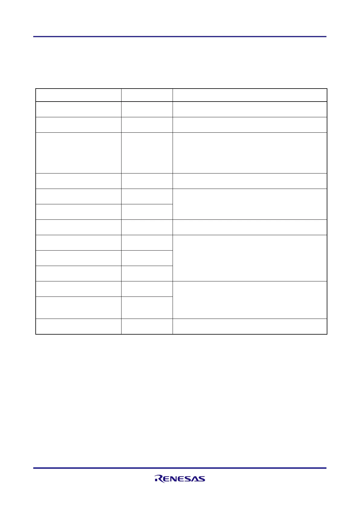
Table 3.1 Device power supply pins (cont'd)
Device power supply pin Voltage Function
E0VCC, E1VCC, E2VCC 3.3 V, 5 V Power supply for I/O ports
LVDVCC 3.3 V, 5 V Power supply for LVDS ports
SYSVCC 3.3 V, 5 V Power supply for
• System Logic and internal voltage regulator power
• I/O ports
VCC 3.3 V, 5 V Power supply for on-chip flash memory
SVRDRVCC 3.3 V, 5 V Power supply for on-chip Switching Voltage Regulator (SVR)
SVRAVCC 3.3 V, 5 V
VDDIOF 3.3 V, 5 V I/O voltage supply for the Main Board
GETH0PVCC 3.3 V, 5V Power supply for Ethernet domain (for U2A16 only)
GETH0BVCC 3.3 V, 5V
GETH0RVCC 3.3 V, 5V
A0VCC, A1VCC, A2VCC 3.3 V, 5 V A/D Converter's power supplies and reference voltages
A0VREFH, A1VREFH,
A2VREFH,
3.3 V, 5 V
VDD 1.12 V * Core supply voltage
Note: * Refer to 3.3 Device Core Voltage (VDD) Selection for further details about VDD voltage.
Each of the above voltages can be selected from
• 5.0 V, 3.3 V (where applicable, see table above)
by a set of jumpers. For details refer to the figure below and
Table 2.1 Jumpers overview
(cont'd).

 Loading...


