RH850/U2A 292pin 8. Jumper Configuration Examples
R20UT4970ED0101 Rev.1.01 Page 54 of 67
July 08, 2022
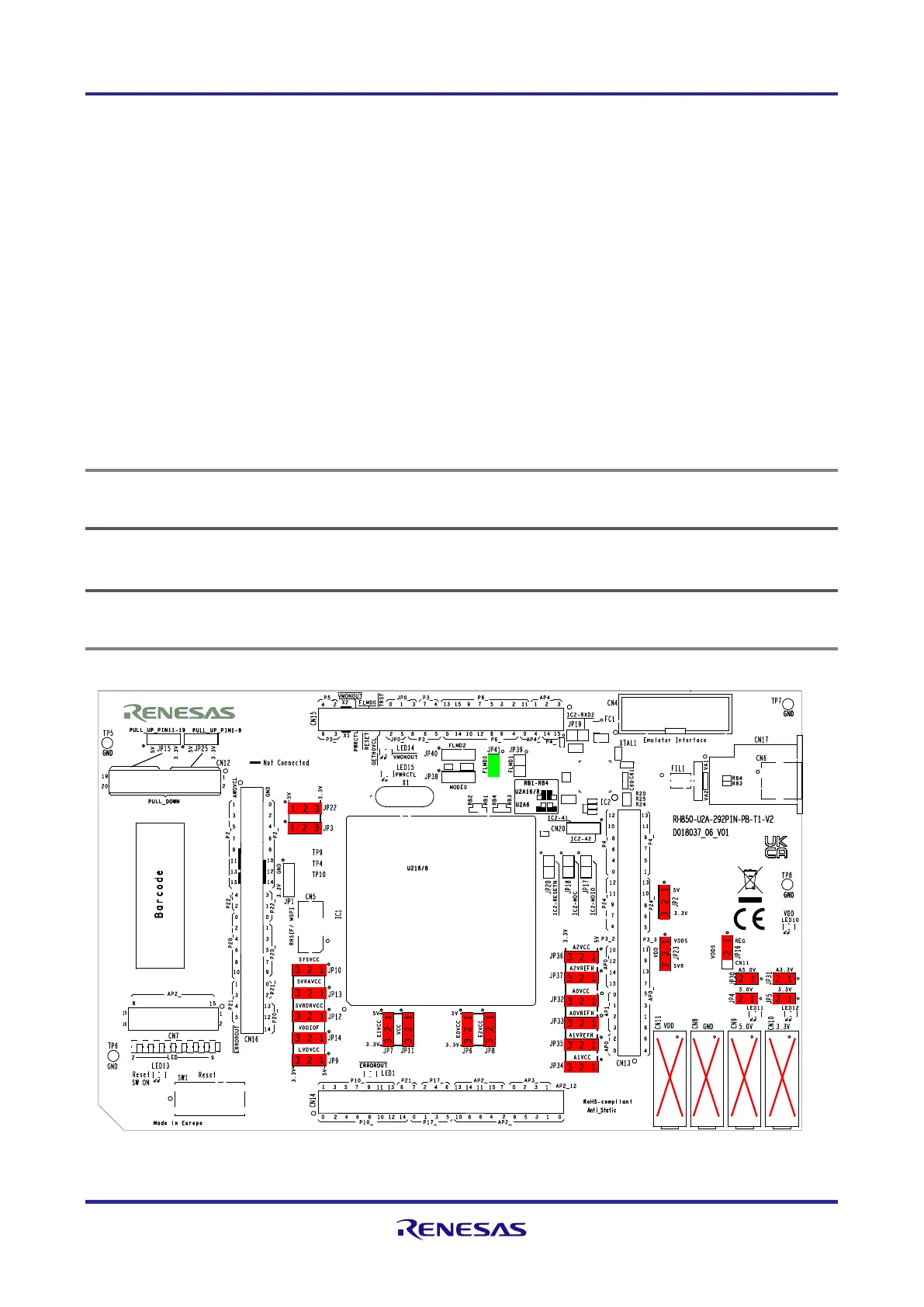
8.2.5 Operation on the Main Board: No External Supply
This example assumes the piggyback board is plugged onto a Main Board, which provides
3.3 V and 5.0 V.
Do not supply the 5V (CN9) and 3.3V (CN10) voltage directly to the piggyback board
• CN8 to CN11: not connected, no external 5.0 V, 3.3 V, 1.12 V
• select desired 3.3 V/5.0 V via jumpers JP2, JP3, JP6 to JP14, JP22 and JP32 to JP3
Refer to 3.2Voltage Distribution for further details about VDD voltage and possible settings of jumpers JP2, JP3
and JP22.
• VDD supply:
− JP16[2-1]: use reg_vcc_VDD from on-board voltage regulator for supply of VDD voltage
− VDD from reg_vcc_VDD (JP23[2-1]) or SVR_OUTPUT (JP23[2-3]) from on-chip Switching Voltage
Regulator
Refer to 3.3 Device Core Voltage (VDD) Selection for further details about VDD voltage.
Note
This configuration still allows to utilize an external IN_1v12 voltage (connected to CN8, CN11) as the source
for VDD voltage. In this case set JP16[2-3] and JP23[2-1].
CAUTION
Do not supply 5V (CN9) and 3.3V (CN10) directly to the piggyback board if these voltages are already
supplied by the main board.
8.3 Main board operation without external power supply

 Loading...


