RH850/U2A 292pin 8. Jumper Configuration Examples
R20UT4970ED0101 Rev.1.01 Page 52 of 67
July 08, 2022
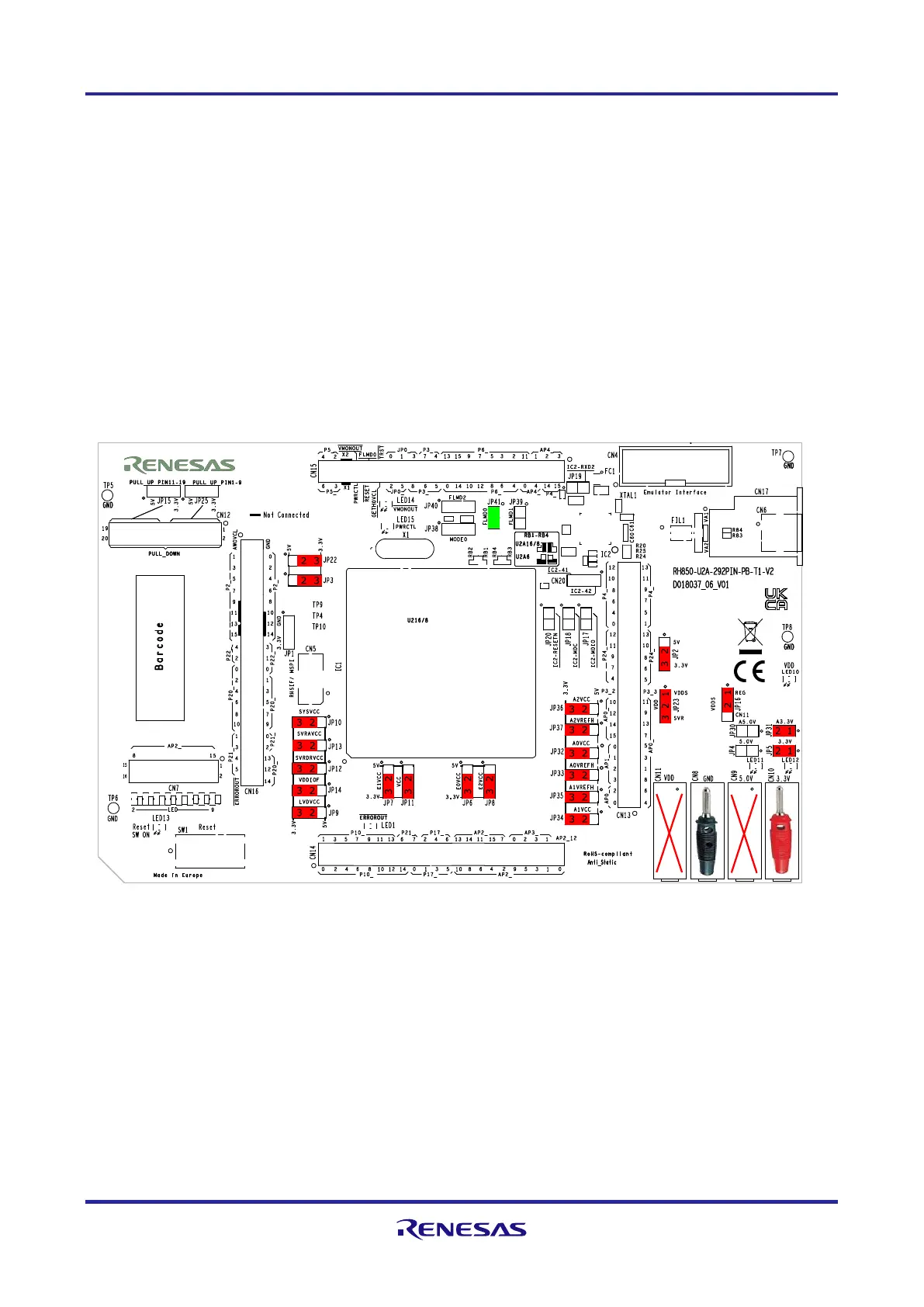
8.2.3 Stand-Alone Operation with Single External Power Supply: Minimum Configuration
This example enables to operate the board with only the 3.3 V external power supply.
Since no 5 V voltage is available, all I/O ports can only use 3.3 V.
• CN8: GND connection
• CN9: not connected, no 5.0 V
− jumpers JP2, JP3, JP6 to JP14, JP22 and JP32 to JP37 are set to 3.3 V position [2-3]
• CN10: 3.3 V
• CN11: not connected, no IN_1v12
− JP16[2-1]: use reg_vcc_VDD from on-board voltage regulator for supply of VDD voltage
− VDD from reg_vcc_VDD (JP23[2-1]) or from SVR_OUTPUT (JP23[2-3]) from on-chip Switching Voltage
Regulator
Refer to 3.3 Device Core Voltage (VDD) Selection for further details about VDD voltage.
8.1 Stand-alone operation with minimum external power supply

 Loading...


