Rockwell Automation Publication 20D-PM001D-EN-P - March 2019 93
Programming and Parameters Chapter 2
545 Bus Reg Ki
Sets the responsiveness of the bus regulator.
Note: This parameter was added for firmware version 2.003.
Default:
Min/Max:
450.0
0.0/100000
RW 16-bit
Integer
546 Bus Reg Kp
Proportional gain for the bus regulator. Used to adjust regulator response.
Note: This parameter was added for firmware version 2.003.
Default:
Min/Max:
1500.0
0.0/10000.0
RW 16-bit
Integer
547 Bus Reg Kd
Derivative gain for the bus regulator. Used to control regulator overshoot.
Note: This parameter was added for firmware version 2.003.
Default:
Min/Max:
1000.0
0.0/10000.0
RW 16-bit
Integer
548 Bus Reg ACR Kp
This proportional gain, in conjunction with Par 545 [Bus Reg Ki], adjusts the output frequency of the drive
during a bus limit or inertia ride through condition. The output frequency is adjusted in response to an error in
the active, or torque producing, current to maintain the active bus limit, or inertia ride through bus reference. A
larger value of gain reduces the dynamic error of the active current.
Note: This parameter was added for firmware version 2.003.
Default:
Min/Max:
225.0
0.0/100000
RW 16-bit
Integer
549 Vuv Fdbk Offset
Displays the motor U phase to V phase offset voltage from the voltage feedback circuit. The value of the offset
is a uni-polarity signal. A zero offset is equal to 16384.
Note: This parameter was added for firmware version 3.001.
Default:
Min/Max:
16384.0
15764.0/17004.0
RW 16-bit
Integer
550 Vvw Fdbk Offset
Displays the motor V phase to W phase offset voltage from the voltage feedback circuit. The value of the offset
is a uni-polarity signal. A zero offset is equal to 16384.
Note: This parameter was added for firmware version 3.001.
Default:
Min/Max:
16384.0
15764.0/17004.0
RW 16-bit
Integer
551 CurrFdbk AdjTime
Compensates for current feedback delays in High Horse Power drives (frames 9 and up).
Note: This parameter was added for firmware version 3.001.
Default:
Min/Max:
Units:
0.0
0.0/50.0
μs
RW 16-bit
Integer
552 Slip Preload Val
The Slip Gain value to be pre-loaded if the drive is powered down.
Note: This parameter was added for firmware version 3.001.
Default:
Min/Max:
120.0
0.0/8192.0
RW 32-bit
Integer
553 Slip Slew Rate
Sets the rate at which the Slip Gain Regulator output transitions from the inactive state to the active state.
Notes: This parameter was added for firmware version 3.001. The default value was changed from “2.000” to
“0.200” for firmware version 4.001.
Default:
Min/Max:
Units:
0.200
0.010/16.383
μs
RW Real
554 LED Status
Used to monitor LED statuses including the main controller, SynchLink and DriveLogix5370 from a HIM or an application program (e.g., DriveExplorer™). This feature is only available with DriveLogix
version 15.03 or later.
• Bit 0 “Sts Active” - Drive running, no faults are present.
• Bit 1 “Sts Ready” - Drive ready, but not running & no faults are present.
• Bit 2 “Sts HW Fault” - A non-resettable fault has occurred in the drive.
• Bit 3 “Sts Fault” - A fault has occurred in the drive.
• Bit 4 “Sts Alarm” - A type 1 (user configurable) alarm condition exists, but the drive continues to run.
• Bit 5 “Sts RunInhbt” - A type 2 (non-configurable) alarm condition exists, drive continues to run.
• Bit 6 “Sync InSync” - The module is configured as the time keeper or the module is configured as a follower and synchronization is complete.
• Bit 7 “Sync NotSync” - The follower(s) are not configured with the time keeper.
• Bit 8 “DL Run Mode” - The controller is in “Run” mode.
• Bit 9 “DL Force Act” - I/O forces are active (enabled) but may or may not exist.
• Bit 10 “DL ForceNtEn” - One or more input or output addresses have been forced to an On or Off state, but the forces have not been enabled.
• Bit 11 “DL Battery” - Either the battery is not installed or 95% discharged and should be replaced.
• Bit 12 “DL I/O Activ” - The controller is communicating with all the devices in its I/O configuration.
• Bit 13 “DL I/O Alarm” - One or more devices in the I/O configuration of the controller are not responding.
• Bit 14 “DL I/O Fault” - The controller is not communicating to any devices and is faulted.
• Bit 15 “DL ComActive” - RS-232 activity.
• Bit 16 “DL Fault” - The controller detected a non-recoverable fault, so it cleared the project from memory.
• Bit 17 “DL NotActive” - If the controller is a new, then it requires a firmware update, or if the controller is not new, a major fault occurred.
• Bit 18 “DL OK” - Controller is OK.
• Bit 19 “DL Loading” - The controller is storing or loading a project to or from nonvolatile memory.
• Bit 20 “DL CF Flash” - The controller is reading from or writing to the CompactFlash™ card.
• Bit 21 “DL CF Format” - The CompactFlash memory is not initialized.
• Bit 22 “DL CF Error” - CompactFlash card does not have a valid file system.
Note: This parameter was added for firmware version 3.001.
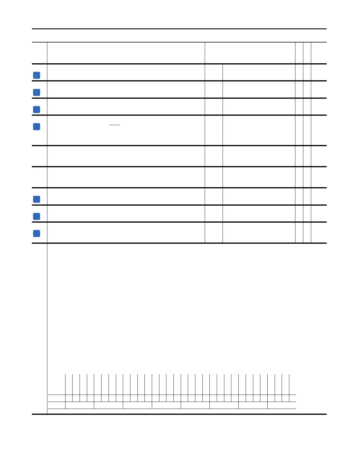
No. Name
Description
Values
Linkable
Read-Write
Data Type
Options
Reserved
Reserved
Reserved
Reserved
Reserved
Reserved
Reserved
Reserved
Reserved
DL CF Error
DL CF Format
DL CF Flash
DL Loading
DL OK
DL NotActive
DL Fault
DL ComActive
DL I/O Fault
DL I/O Alarm
DL I/O Activ
DL Battery
DL ForceNtEn
DL Force Act
DL Run Mode
Sync NotSync
Sync InSync
Sts RunInhbt
Sts Alarm
Sts Fault
Sts HW Fault
Sts Ready
Sts Active
Default xxxxxxxxx00000000000000000000000
Bit 313029282726252423222120191817161514131211109876543210
0 = False
1 = True
 Loading...