AR-M207 M165 M162 ELECTRICAL SECTION 13-3
96 PF0/BREQ Out 151 Selector Signal
97 P50/TxD2/IRQ4 Out IMC2 Status Transmission
98 P51/RxD2/IRQ5 In IMC2 Status Reception
99 Vss GND Ground
100 Vss GND Ground
101 P52/SCK2/IRQ6 In IMC2 Status Transmission
Enable
102 P53/ADTRG/
IRQ7/WAIT/
BREQO
Out IMC2 Status Reception Ready
103 Avcc 3.3V A/D Power
104 Vref 3.3V A/D Reference
105 P40/AN0 In Thermistor Analog Input
106 P41/AN1 In SPF Wide Sensor
107 P42/AN2 In 151 Selector Input
108 P43/AN3 In 151 Selector Input
109 P44/AN4 In 151 Selector Input
110 P45/AN5 In 151 Selector Input
111 P46/AN6/DA0 In Not use
112 P47/AN7/DA1 In Analog Input(TC)
113 Avss GND Ground
114 Vss GND Ground
115 P17/PO15/
TIOCB2/TCLKD
Out Scan stop Signal
No. SIGNAL In/Out DESCRIPTION
116 P16/PO14/
TIOCA2
Out Scan start Signal
117 P15/PO13/
TIOCB1/TCLKC
Out Trans start Signal
118 P14/PO12/
TIOCA1
Out Polygon Motor Clock
119 P13/PO11/
TIOCD0/TCLKB
Out SPF Motor Drive
120 P12/PO10/
TIOCC0/TCLKA
Out SPF Motor Drive/Mirror Motor
Step count
121 P11/PO9/
TIOCB0/DACK1
Out SPF Motor Drive
122 P10/PO8/
TIOCA0/DACK0
Out SPF Motor Dribe
123 MD0 GND CPU Mode Control
Input(Mode4)
124 MD1 GND CPU Mode Control
Input(Mode4)
125 MD2 Pull-Up CPU Mode Control
Input(Mode4)
126 PG0/CAS Out Not use
127 PG1/CS3 Out ChipSelect for I/O ASI
128 PG2/CS2 Out ChipSelect for ASIC
No. SIGNAL In/Out DESCRIPTION
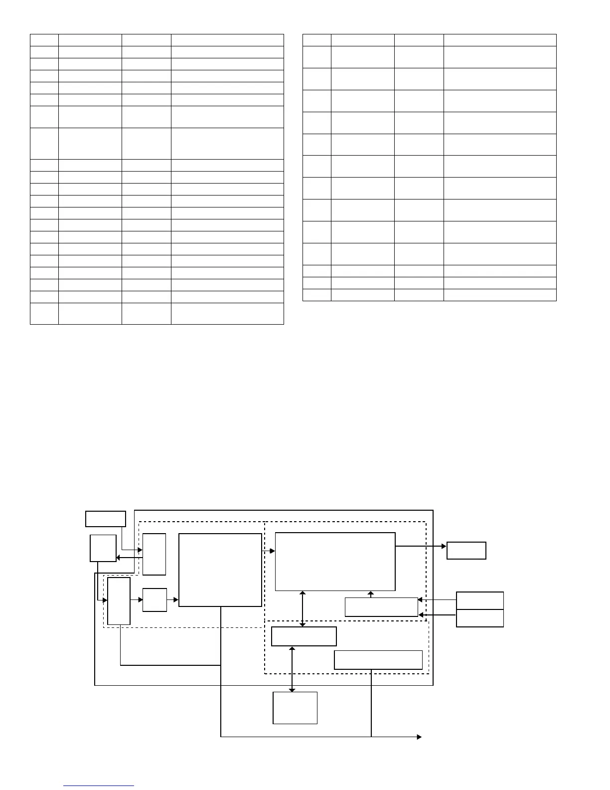
(3) Image process ASIC (HG73C141HFV)
a. General
The ASIC is composed of the three major blocks: the image process section, the print control section, and the I/F section.
•Image process section:
With image data from the CCD PWB in the operation mode determined by the register setup, shading, AE process, input γ correction, area separation,
filter process, resolution conversion, zoom process, output γ correction, binary conversion (error diffusion, dither method, simple binary conversion) are
performed.
•Print control section:
When copying, the image-processed data are outputted to the LSU according to the LSU writing timing. When scanning, the image data are made into
8bit width and outputted to the I/F section (USB).
•I/F section:
Controls the DRAM which is the image data buffer, and processes data send/receive between the USB I/F and the IEEE1284 I/F.
The ASIC is controlled by writing the operation mode and the necessary setup values of the operation mode into the ASIC control register before
starting each operation. (For ASIC Pin configuration, refer to the table at the end of this document.)
Scan start
CCD
PWB
Shading
CCD drive
AE
Resolution conversion,
Zooming, lmage
process circuit
Print data process circuit
DRAM control
PRINT control
DRAM
8MB or 16MB
LSU
HSYNC
VSYNC
To CPU bus
ASIC
Image process section
I/F section
Print control section
ASIC control resistor
[13]ELECTRICALSECTION.fm 3 ページ 2004年11月12日 金曜日 午後2時21分