-
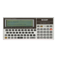
PC-1600
3. Block diagram
0
0
-
0,
8
0
0
-
0
7
R!W
1ff' ~
ERASE
FDC
&
WO
LOGIC
f--;l
A
o
- A,
3
A
o
-
A,
WG
R!W AMP
~
LSI
RD
FROM
~
GATE
CE·1600P
ARREY
{PRINTER)
107N, WR, RD,
3
CSO, WR, RD,
SOLENOID
r
j
RSTN
REST
SOLENOID
~
POWER ON
,
CONTROL
RESET
CIRCUIT
CIRCUIT
Vcc (+5V) +5V
~
5VB
rr1
REGURATED
~
POWER
SUPPLY
5VC
CIRCUIT
MOTOR
CONTROL
Vp (+6V)
+6V
CIRCUIT
50P CONNECTOR
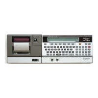
FDU-250 MICRO FLOPPY DISK DRIVE UNIT
4. Circuit description
POWER ON
4-1. Internal operation
Since the floppy disk controller is contained within the
2.5" floppy disk drive unit and directly interfaced with the
bus line, data line and control signals are directly con-
nected.
So, only the power-on-reset signal generation circuit and
the amp's 5VC (+5V) supply regulator circuit are provided
for circuit.
I
I
VCC
~y
VCC
I
(+5)
, 0
Delay
-:---+/lJ.
H
@ ::
L
____
.;__-;
, System reset
4-2. Power-on-reset signal generation circuit
, ,
Reset ~
n
t
period~ U
H
L
VCC
VCC
Fig.2 Raset timings
R5
RSTN
REST
Fig. 1 shows the reset circuit and Fig. 2 shows its timings.
R5 is acharge current regulating resistor C3 which is used
for pullup and delay. D4 is a diode which is used to bypass
the charge in C3 to VCC line when VCC is off.
Fig. 1 Raset circuit
-99-