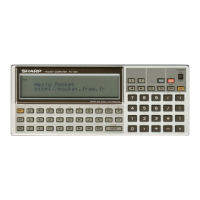
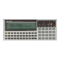
3. Description of each block
3-1. LR38045 gate array
Table below shows the functions and port address of the
gate array block.
Block
Function
Bu
A bidirectional 8-bit
Input/output
buffer.
(8-bit
1/0
buffer)
Mu Used to select FF1, FF2, FF3, or PA port
(multiplexer)
when data are read from the gate
arrav.
FF1~FF3
FF1: The
interrupt circuit
is ControlIed with
(S-bit latch)
an FFl
outpur.
For instance, when a
certain bit is
set
to
"1",
the
Input
signal to the PA
port
(PAO~61
I
which
corresponds to the bit is sent on the
IRQ llne asan interrupt signal.
FF2: PB
port
(PSO~7Nllatch
FF3:
PC
port
(PCO~7Nllatch
DC1~3
DCl : For generation of 32KS ROM chip
(decoder)
select signal. (CSNO)
DC2: For generation of 2.5" FDD select
signal. (I07N)
DC3: For selection of FFl ~FF3
and
FFD
reset latch at the time of data write.
Or selection of FFl ~FF3 or PA port
at the time of data read.
INT
Inputs to the PA port (PAO~611 are ORed
(Interrupt
circuit)
and sent on the IRQ line asan
interrupt
signal.
As PAO~61 correspond to QO~Q6 of FF1,
the i
nterrupt
is enabled when FF
1
is
set
with "1".
(Fig. 3 shows the quivalent circuit of the
interrupt
circuit.)
IRQ
p
~
r;;;::-r-
QO
PAOI
QI
PAlI
Q2
PA21
Q8
PA81
Q4 PA.41
Q6
PAS I
Q6
PA61
'----
To multiplexer
(Fig. 3)
Interrupt
circuit
RST FFl ~3 are reset by this
circuit,
when
a
reset
(reset circuitl
signal is received on RSTI.
At the sametime, the 2/5" FDD reset signal
(RSTN) is issuedwhich will be keot active
until cleared by software.
_L....
-65-
-
PC-l600
Block
Function
It is possible without an input on RST! to
outpur RSTN by msans öf sottware.
(Fig. 4 shows the equivalent circuit of the
reset
circuit and Fig. 5 shows its timings.)
R$TN
·RSTE.
'l1li1
0
'"
[)o
I
I •
IFrom PC-1600) ~ .. FFl
-3
RESET
(Fig. 41 Reset
circuit
JlSTE___n
~=============
OD.
RSTN
~
Software reset
(Fig. 51 Reset circuit timings
CMT I/F
I
The cassettesignal received from the EAR
(cassette
interface jack isamplified and waveform
shaped,
circuitl to be sent on PA78. (SeeFig.6 for its
equivalent circuit.1
EAR----tl .........._.!. : ~
~
fU1Jl
.
.
~---------
-----------~
(Fig. 6) Cassetteinterface circuit equivalent
circuit
NOTE: Ports, PA, PB, and PC, are all active high within
the gate arrav, but they are converted to active
low signals outside of the gate
arrav,
Gate array
I
Inside
I
Outside
I
PAO-61
PBON~7N
PCON-7N
ACTIVE HIGH
AcTIVE lOW
For instance, if "1" is set to 00 of FF2, the
PBONoutpur becomes low.