8-47
System Manual
C79000-G8576-C199-06
F+
F–
1
2
4
6
8
10
12
14
16
18
20
25
27
29
31
33
35
37
39
41
g
g
g
g
g
g
g
g
LED Pin
Shield
t
t
t
t
t
t
t
t
t
+5V
1N1N
2N2N
3N3N
4N4N
1I0.0
1L
2I0.1
2L
3I0.2
3L
4I0.3
4L
1)
x20
2)
5N5N
6N6N
7N7N
8N8N
5I0.45L
6I0.56L
7I0.67L
8I0.78L
2)
(6)
I
0.5
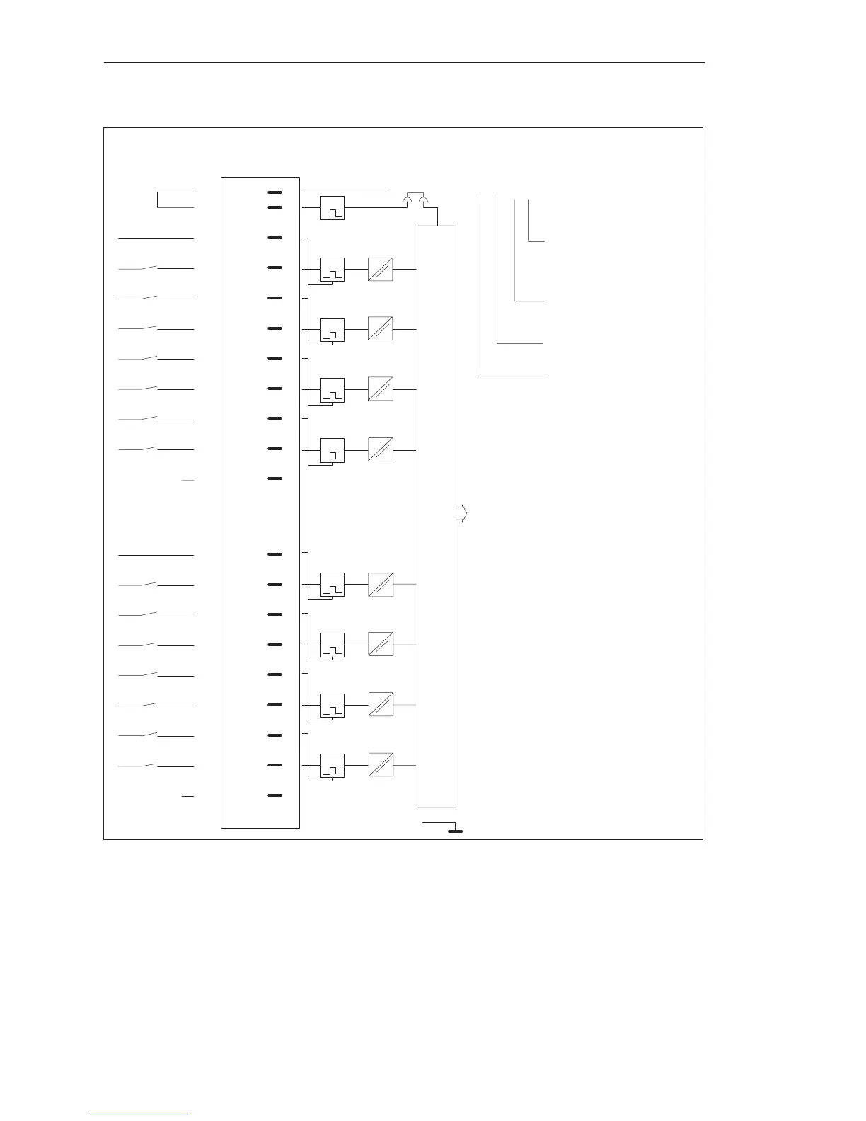
Front StripConnection of
Process Signal
Lines
Example of connection designation for
an input:
Input 5 (5th bit);
0 to 7 possible
Address of input byte
(byte 0);
0 to 255 possible
I = Input
6th group (not speci-
fied in the address)
Block Diagram of
Module Inputs
Data Memory and S5 Bus Control
g = Green LED (status indicator)
F+/F- = Enable input (jumper in front connector)
1)
Changeover of enable mode with jumper X20:
Jumper inserted = Enable input active (factory setting)
Jumper open = Enable input inactive.
2
) The terminal is not connected internally. When this terminal is connected to input voltages, the clearances in air and
leakage paths remain adequate to UL, CSA and VDE.
Di
ital Input/Output Modules
 Loading...