2-32
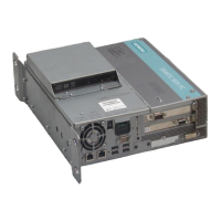
Box PC 820 / PC FI45 V2, Manual
A5E00051531-03
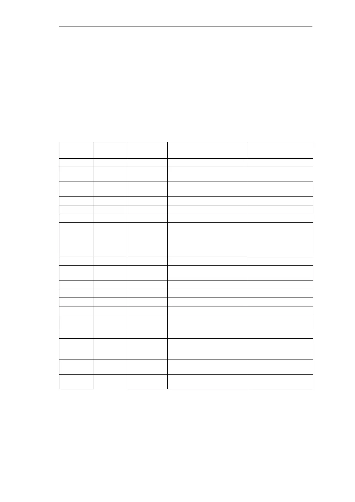
2.10.2 Assignment of the Memory Addresses
There are two kinds of address areas:
S Memory address area
S I/O address area.
Different read/write signals (I/O WR, I/O RD, MEMR, MEMW) are used to
reference these areas. The following tables provide you with an overview of the
address areas used. Please refer to the descriptions of the individual functional
groups for more details.
From
Address
To
Address
Size Assignment Remark
0000 0000 0007 FFFF 512k Conventional system memory
0008 0000 0009 FBFF 127k Conventional system memory
extended
0009 FC00 0009 FFFF 1k Conventional system memory
extended BIOS data
000A 0000 000A FFFF 64k Graphics refresh memory VGA
000B 0000 000B 7FFF 32k SW graphics interface module Vacant
000B 8000 000B FFFF 32k Graphics refresh memory VGA/CGA
000C 0000 000D FFFF 148k VGA BIOS expansion and
system resources. The
available area above 000C
7FFF depends on the system
equipment.
VGA
000E 0000 000E BFFF 48k System BIOS
000E C000 000E CFFF 4k System BIOS
BootMessageLogo
000E D000 000E DFFF 4k System BIOS Plug & Play Area
000E E000 000E FFFF 8k System BIOS Boot Block
000F 0000 000F FFFF 64k System BIOS
0010 0000 00EF FFFF 14M Extended system memory
00F0 0000 00FF FFFF 1M Extended system memory or
Memory hole
Via BIOS SETUP
0100 0000 2FFF FFFF 768M Extended system memory
3000 0000 FFEF FFFF 4G-768M-
1023k
PCI expansion; resources are
assigned by the operating
system.
FFF0 0000 FFFD FFFF 1023k-128k ISA memory, reserved for dual-
port RAM
Vacant
FFFE 0000 FFFF FFFF 128k Shadow of System BIOS
(000E 0000 .. 000F FFFF)
Motherboard