– 29 –
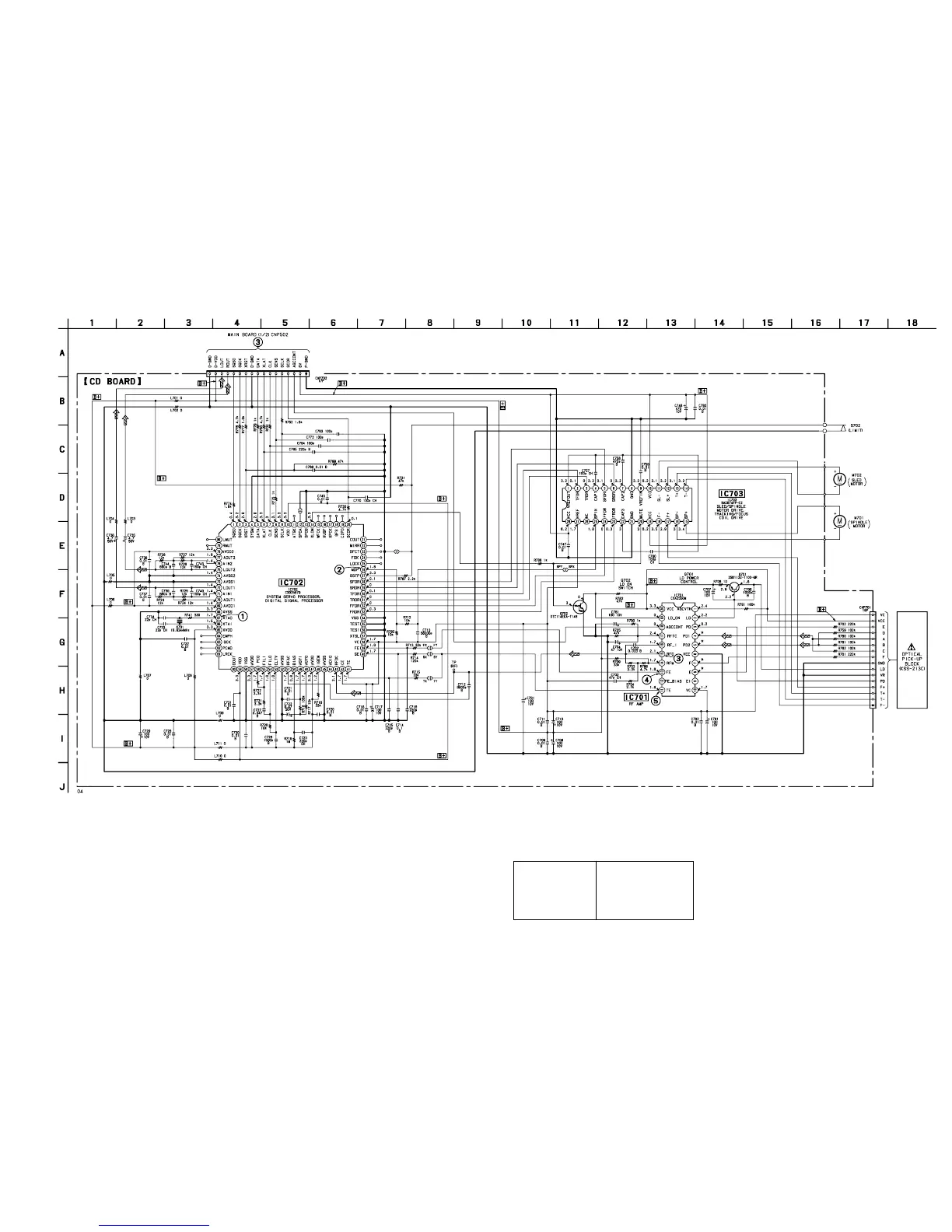
6-8. SCHEMATIC DIAGRAM — CD SECTION — • Refer to page 47 for IC Block Diagrams.
– 30 –
Note on Schematic Diagram:
• All capacitors are in µF unless otherwise noted. pF: µµF
50 WV or less are not indicated except for electrolytics
and tantalums.
• All resistors are in Ω and
1
/
4
W or less unless otherwise
specified.
• U : B+ Line.
Note:
The components identi-
fied by mark 0 or dotted
line with mark 0 are criti-
cal for safety.
Replace only with part
number specified.
Note:
Les composants identifiés par
une marque 0 sont critiques
pour la sécurité.
Ne les remplacer que par une
piéce portant le numéro
spécifié.
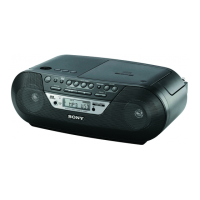
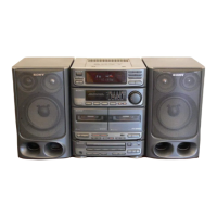
CFD-S22/S32
• Power voltage is dc 9V and fed with regulated dc power
supply from battery terminal.
• Voltage and waveforms are dc with respect to ground
under no-signal (detuned) conditions.
no mark : CD STOP
∗
: Impossible to measure
• Voltages are taken with a VOM (Input impedance 10 MΩ).
Voltage variations may be noted due to normal produc-
tion tolerances.
• Waveforms are taken with a oscilloscope.
Voltage variations may be noted due to normal produc-
tion tolerances.
• Circled numbers refer to waveforms.
• Signal path.
J : CD
(Page 35)