69
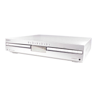
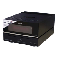
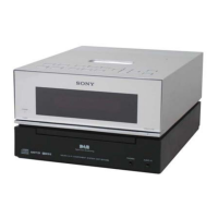
HCD-BC150/BC250
• AMP BOARD IC101 to IC106 CXD9774M (POWER DRIVER)
Pin No. Pin Name I/O Description
1 GND — Power ground
2 PWM_BP I PWM input signal, half-bridge B
3 GND — Power ground
4 RESET I Reset signal
5 DREG_RTN — Decoupling return pin
6 GREG — Local GVDD decoupling pin
7M3IOutput mode selection pin; connect to ground
8 DREG_RTN — Digital supply voltage regulator decoupling pin
9DGND — I/O reference ground
10 M1 I Protection mode selection pin
11 M2 I Protection mode selection pin
12 DVDD — I/O reference supply input
13 SD O Shutdown signal for half-bridges A and B
14 RESV — I/O reference ground
15 OTW O Overtemperature warning output
16 GND — Power ground
17 PWM_AP I PWM input signal, half-bridge A
18 GND — Power ground
19 GREG — Gate drive input voltage
20 GVDD — Gate drive input voltage
21 PVSS — Power ground
22 BST_A —
High side bootstrap supply (BST), external resistor and capacitor to OUT_A
required
23 PVDD_A — Power supply input for half-bridge A
24 PVDD_A — Power supply input for half-bridge A
25 OUT_A O Output, half-bridge A
26 OUT_A O Output, half-bridge A
27 PVSS — Power ground
28 PVSS — Power ground
29 OUT_B O Output, half-bridge B
30 OUT_B O Output, half-bridge B
31 PVDD_B — Power supply input for half-bridge B
32 PVDD_B — Power supply input for half-bridge B
33 BST_B —
High side bootstrap supply (BST), external resistor and capacitor to OUT_B
required
34 PVSS — Power ground
35 GVDD_B — Gate drive input voltage
36 GREG — Gate drive input voltage